Q1 MHT CET 2026 · 15 MAY · SHIFT 1 Easy ☆
Energy Bands in Solids · Conductors, insulators & semiconductors
In semiconductors, at room temperature the
(a) valance band is partially empty and the conduction band is partially filled. (b) valance band is completely filled and the conduction band is partially filled. (c) valance band is completely filled. (d) conduction band is completely empty. Show answer and solution
Answer: (a)
In a semiconductor the band gap is small (about 1 eV 1\text{ eV} 1 eV At room temperature some electrons get thermal energy to jump from the valence band to the conduction band. They leave holes behind, so the valence band is partially empty and the conduction band is partially filled. So the answer is (a). Report a mistake Q2 MHT CET 2026 · 16 APR · SHIFT 2 Easy ☆
Energy Bands in Solids · Conductors, insulators & semiconductors
Electrical conductivity of insulators is
(a) exactly zero (b) extremely large (c) extremely small (d) sometimes small and sometimes large Show answer and solution
Answer: (c)
Insulators have a very large band gap (E g > 3 eV E_g > 3\text{ eV} E g > 3 eV A very few electrons can still be excited, so conductivity is not exactly zero but extremely small. So the answer is (c) extremely small. Report a mistake Q3 MHT CET 2026 · 11 APR · SHIFT 2 Easy ☆
Energy Bands in Solids · Conductors, insulators & semiconductors
In energy band diagram of insulators, a band gap and the conduction band is respectively
(a) very high, empty (b) very low, empty (c) very high, completely filed (d) very low, partially filled Show answer and solution
Answer: (a)
In an insulator the band gap is very large, E g > 3 eV E_g > 3\text{ eV} E g > 3 eV Thermal energy cannot lift electrons across it, so the conduction band is empty. So the answer is (a) very high, empty. Report a mistake Q4 MHT CET 2026 · 13 MAY · SHIFT 1 Medium ☆
Energy Bands in Solids · Conductors, insulators & semiconductors
There is no hole current in good conductors because they
(a) have large forbidden energy gap. (b) have overlapping valence and conduction bands. (c) are full of electrons. (d) have no valence band. Show answer and solution
Answer: (b)
A hole forms only when an electron leaves an otherwise filled valence band across a gap. In good conductors the valence and conduction bands overlap, so there is no gap and no holes are created. So the answer is (b). Report a mistake Q5 MHT CET 2024 · 10 MAY · SHIFT 2 Easy ☆
Energy Bands in Solids · Conductors, insulators & semiconductors
In semiconductors at room temperature,
(a) the valence band is completely filled and the conduction band partially filled. (b) the valence band is completely filled. (c) the conduction band is completely filled. (d) the valence band is partially empty and the conduction band partially filled. Show answer and solution
Answer: (d)
Small band gap (∼ 1 eV \sim 1\text{ eV} ∼ 1 eV This leaves holes in the valence band (partially empty) and electrons in the conduction band (partially filled). So the answer is (d). Report a mistake Q6 MHT CET 2024 · 2 MAY · SHIFT 1 Easy ☆
Energy Bands in Solids · Conductors, insulators & semiconductors
In semiconductors at room temperature,
(a) the valence band is completely filled. (b) the conduction band is completely empty. (c) the conduction band is partially filled and the valence band is partially empty. (d) the valence band is completely filled and conduction band is partially empty. Show answer and solution
Answer: (c)
At room temperature thermal energy excites some electrons across the small gap of a semiconductor. The conduction band becomes partially filled and the valence band partially empty (holes). So the answer is (c). Report a mistake Q7 MHT CET 2023 · 14 MAY · SHIFT 1 Easy ☆
Energy Bands in Solids · Conductors, insulators & semiconductors
In semiconductors at room temperature,
(a) the valence band is completely filled (b) the conduction band is completely filled (c) the condition band is partially filled and valence band is partially empty (d) the valence band is completely filled and the conduction band is partially filled Show answer and solution
Answer: (c)
At room temperature some valence electrons cross the small band gap into the conduction band. So the conduction band is partially filled and the valence band partially empty. So the answer is (c). Report a mistake Q8 MHT CET 2023 · 11 MAY · SHIFT 1 Easy ☆
Energy Bands in Solids · Conductors, insulators & semiconductors
In energy band diagram of insulators, a band gap and the conduction band is respectively
(a) very low and partially filled. (b) very high and completely filled. (c) very high and empty. (d) very low and empty. Show answer and solution
Answer: (c)
Insulators have a very large band gap (E g > 3 eV E_g > 3\text{ eV} E g > 3 eV No electrons can cross it, so the conduction band is empty. So the answer is (c) very high and empty. Report a mistake Q9 MHT CET 2023 · 10 MAY · SHIFT 1 Easy ☆
Energy Bands in Solids · Conductors, insulators & semiconductors
(a) valence band is empty and conduction band is filled with electrons. (b) conduction band is empty and valence band is completely filled with electrons. (c) valence band is partially filled. (d) conduction band is partially filled with electrons. Show answer and solution
Answer: (b)
In an insulator all valence electrons are tightly bound, so the valence band is completely filled. The large gap keeps electrons from reaching the conduction band, so it stays empty. So the answer is (b). Report a mistake Q10 NEET 2023 Easy ☆
Energy Bands in Solids · Conductors, insulators & semiconductors
On the basis of electrical conductivity, which one of the following materials has the smallest resistivity?
(a) Germanium (b) Silver (c) Glass (d) Silicon Show answer and solution
Answer: (b)
Resistivity is smallest for a good conductor. Silver is a metal (best conductor); Ge and Si are semiconductors; glass is an insulator. So the answer is (b) Silver. Report a mistake Q11 MHT CET 2021 · 24 SEP · SHIFT 2 Easy ☆
Energy Bands in Solids · Conductors, insulators & semiconductors
Choose the correct statement. In conductors
(a) valance band and conduction band overlap each other. (b) valance band and conduction band are separated by large energy gap. (c) valancè band and conduction band are separated by a small energy gap. (d) a very small number of electrons are available for electrical conduction. Show answer and solution
Answer: (a)
In conductors (metals) the valence and conduction bands overlap; there is no band gap. So a large number of free electrons is always available for conduction. So the answer is (a). Report a mistake Q12 MHT CET 2021 · 22 SEP · SHIFT 2 Easy ☆
Energy Bands in Solids · Conductors, insulators & semiconductors
Choose the correct statement. In semiconductors valance band and conduction band
(a) is separated by large energy gap. (b) is separated by small energy gap: (c) is almost empty. (d) overlap each other. Show answer and solution
Answer: (b)
Semiconductors have a small band gap, about 1 eV 1\text{ eV} 1 eV 1.1 eV 1.1\text{ eV} 1.1 eV 0.7 eV 0.7\text{ eV} 0.7 eV Large gap means insulator; overlapping bands means conductor. So the answer is (b) separated by a small energy gap. Report a mistake Q13 MHT CET 2021 · 20 SEP · SHIFT 2 Easy ☆
Energy Bands in Solids · Conductors, insulators & semiconductors
In the case of insulators, a band gap and conduction band is respectively
(a) very high empty. (b) very low, partially filled (c) very high, completely filled (d) very low, empty. Show answer and solution
Answer: (a)
Insulators: band gap very large (> 3 eV > 3\text{ eV} > 3 eV Electrons cannot cross it, so the conduction band is empty. So the answer is (a) very high, empty. Report a mistake Q14 MHT CET 2021 · 22 SEP · SHIFT 1 Medium ☆
Energy Bands in Solids · Conductors, insulators & semiconductors
Choose the FALSE statement from the following.
(a) Generally, in conductors the valence and conducting bands overlap. (b) The resistivity of a semiconductor increases with increase in temperature (c) The conductivity of a semiconductor increase with increase in temperature (d) Substances with energy gap of the order of 10 eV 10\text{ eV} 10 eV Show answer and solution
Answer: (b)
(a) True: in conductors the bands generally overlap. (b) False: resistivity of a semiconductor decreases as temperature rises (more electron-hole pairs). (c) True: conductivity increases with temperature. (d) True: E g ∼ 10 eV E_g \sim 10\text{ eV} E g ∼ 10 eV So the false statement is (b). Report a mistake Q15 NEET 2012 · AIPMT · PRELIMS Medium ☆
Energy Bands in Solids · Conductors, insulators & semiconductors
C and Si both have same lattice structure; having 4 bonding electrons in each. However, C is insulator where as Si is intrinsic semiconductor. This is because
(a) In case of C the valence band is not completely filled at absolute zero temperature. (b) In case of C the conduction band is partly filled even at absolute zero temperature. (c) The four bonding electrons in the case of C lie in the second orbit, whereas in the case of Si they lie in the third. (d) The four bonding electrons in the case of C lie in the third orbit, whereas for Si they lie in the fourth orbit. Show answer and solution
Answer: (c)
C (1 s 2 2 s 2 2 p 2 1s^2 2s^2 2p^2 1 s 2 2 s 2 2 p 2 … 3 s 2 3 p 2 \ldots 3s^2 3p^2 … 3 s 2 3 p 2 Electrons in the 2nd orbit are closer to the nucleus and more tightly bound, so the band gap of C (about 5.4 eV 5.4\text{ eV} 5.4 eV 1.1 eV 1.1\text{ eV} 1.1 eV Hence C is an insulator and Si a semiconductor. So the answer is (c). Report a mistake Q16 JEE Main 2007 · AIEEE Medium ☆
Energy Bands in Solids · Conductors, insulators & semiconductors
Carbon, silicon and germanium have four valence electrons each. At room temperature which one of the following statements is most appropriate?
(a) The number of free electrons for conduction is significant only in Si \text{Si} Si Ge \text{Ge} Ge C . \text{C}. C . (b) The number of free conduction electrons is significant in C \text{C} C Si \text{Si} Si Ge . \text{Ge}. Ge . (c) The number of free conduction electrons is negligibly small in all the three. (d) The number of free electrons for conduction is significant in all the three Show answer and solution
Answer: (a)
Band gaps: C ≈ 5.4 eV \approx 5.4\text{ eV} ≈ 5.4 eV 1.1 eV 1.1\text{ eV} 1.1 eV 0.7 eV 0.7\text{ eV} 0.7 eV k T ≈ 0.025 eV kT \approx 0.025\text{ eV} k T ≈ 0.025 eV Small gaps of Si and Ge allow a significant number of electrons to be thermally excited; the large gap of C allows almost none. So the answer is (a). Report a mistake Q17 JEE Main 2006 · AIEEE Medium ☆
Energy Bands in Solids · Band formation & band gap
If the lattice constant of this semiconductor is decreased, then which of the following is correct?
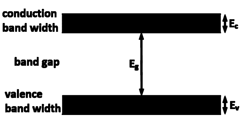
(a) All E c , E g , E v E_c, E_g, E_v E c , E g , E v (b) E c E_c E c E v E_v E v E g E_g E g (c) E c E_c E c E v E_v E v E g E_g E g (d) All E c , E g , E v E_c, E_g, E_v E c , E g , E v Show answer and solution
Answer: (c)
In the figure E c E_c E c E v E_v E v E g E_g E g Smaller lattice constant means atoms are closer, so their wave functions overlap more. Greater overlap spreads each level over a wider range: E c E_c E c E v E_v E v Wider bands come closer to each other, so the gap E g E_g E g This gives (b); the answer key gives (c). Report a mistake Q18 NEET 2005 · AIPMT Easy ☆
Energy Bands in Solids · Conductors, insulators & semiconductors
Choose the only false statement from the following.
(a) In conductors the valence and conduction bands overlap. (b) Substances with energy gap of the order of 10 eV are insulators. (c) The resistivity of a semiconductor increases with increase in temperature. (d) The conductivity of a semiconductor increases with increase in temperature. Show answer and solution
Answer: (c)
(a) True: in conductors the bands overlap. (b) True: E g ∼ 10 eV E_g \sim 10\text{ eV} E g ∼ 10 eV 3 eV 3\text{ eV} 3 eV (c) False: as T T T (d) True: conductivity increases with temperature. So the false statement is (c). Report a mistake Q19 NEET 2005 · AIPMT Easy ☆
Energy Bands in Solids · Conductors, insulators & semiconductors
Carbon, silicon and germanium atoms have four valence electrons each. Their valence and conduction bands are separated by energy band gaps represented by (Eg)C, (Eg)si and (Eg)Ge respectively. Which one of the following relationships is true in their case?
(a) (Eg)C > (Eg)Si (b) (Eg)C < (Eg)Si (c) (Eg)C = (Eg)Si (d) (Eg)C < (Eg)Ge. Show answer and solution
Answer: (a)
Band gaps: carbon (diamond) E g ≈ 5.4 eV E_g \approx 5.4\text{ eV} E g ≈ 5.4 eV 1.1 eV 1.1\text{ eV} 1.1 eV 0.7 eV 0.7\text{ eV} 0.7 eV So ( E g ) C > ( E g ) S i > ( E g ) G e (E_g)_C > (E_g)_{Si} > (E_g)_{Ge} ( E g ) C > ( E g ) S i > ( E g ) G e So the answer is (a) ( E g ) C > ( E g ) S i (E_g)_C > (E_g)_{Si} ( E g ) C > ( E g ) S i Report a mistake Q20 JEE Main 2005 · AIEEE Medium ☆
Energy Bands in Solids · Band formation & band gap
The electrical conductivity of a semiconductor increases when electromagnetic radiation of wavelength shorter than 2480 nm 2480\text{ nm} 2480 nm ( eV ) (\text{eV}) ( eV )
(a) 2.5 eV 2.5\text{ eV} 2.5 eV (b) 1.1 eV 1.1\text{ eV} 1.1 eV (c) 0.7 eV 0.7\text{ eV} 0.7 eV (d) 0.5 eV 0.5\text{ eV} 0.5 eV Show answer and solution
Answer: (d)
Conductivity rises only when photon energy ≥ E g \ge E_g ≥ E g E g = h c λ m a x E_g = \dfrac{hc}{\lambda_{max}} E g = λ ma x h c E g ( eV ) = 1240 λ ( nm ) = 1240 2480 E_g(\text{eV}) = \dfrac{1240}{\lambda(\text{nm})} = \dfrac{1240}{2480} E g ( eV ) = λ ( nm ) 1240 = 2480 1240 E g = 0.5 eV E_g = 0.5\text{ eV} E g = 0.5 eV So the answer is (d) 0.5 eV 0.5\text{ eV} 0.5 eV Report a mistake Q21 JEE Main 2004 · AIEEE Easy ☆
Energy Bands in Solids · Band formation & band gap
The manifestation of band structure in solids is due to
(a) Bohr's correspondence principle (b) Pauli's exclusion principle (c) Heisenberg's uncertainty principle (d) Boltzmann's law Show answer and solution
Answer: (b)
When atoms come together in a solid, their identical energy levels cannot hold the same electrons in the same state. Pauli's exclusion principle forces each level to split into many closely spaced levels, which form a band. So the answer is (b) Pauli's exclusion principle. Report a mistake Q22 NEET 2004 · AIPMT Easy ☆
Energy Bands in Solids · Conductors, insulators & semiconductors
In semiconductors at a room temperature
(a) the valence band is partially empty and the conduction band is partially filled (b) the valence band is completely filled and the conduction band is partially filled (c) the valence band is completely filled (d) the conduction band is completely empty Show answer and solution
Answer: (a)
At room temperature some electrons cross the small gap of a semiconductor. Valence band becomes partially empty (holes) and conduction band partially filled. So the answer is (a). Report a mistake Q23 JEE Main 2002 · AIEEE Easy ☆
Energy Bands in Solids · Conductors, insulators & semiconductors
The energy band gap is maximum in
(a) metals (b) superconductors (c) insulator (d) semiconductor Show answer and solution
Answer: (c)
Metals and superconductors: bands overlap, E g = 0 E_g = 0 E g = 0 Semiconductors: E g ≈ 1 eV E_g \approx 1\text{ eV} E g ≈ 1 eV E g > 3 eV E_g > 3\text{ eV} E g > 3 eV So the answer is (c) insulator. Report a mistake Q24 MHT CET 2026 · 14 MAY · SHIFT 2 Easy ☆
Intrinsic & Extrinsic Semiconductors · Intrinsic semiconductors
In an intrinsic semiconductor, at any ordinary temperature, the correct relation between the number of electrons per unit volume (n e n_e n e n h n_h n h
(a) n e = n h n_e = n_h n e = n h (b) n e > n h n_e > n_h n e > n h (c) n e < n h n_e < n_h n e < n h (d) n e = n h = 0 n_e = n_h = 0 n e = n h = 0 Show answer and solution
Answer: (a)
In an intrinsic semiconductor every broken covalent bond gives one free electron and one hole. So n e = n h = n i n_e = n_h = n_i n e = n h = n i So the answer is (a) n e = n h n_e = n_h n e = n h Report a mistake Q25 MHT CET 2026 · 18 APR · SHIFT 2 Easy ☆
Intrinsic & Extrinsic Semiconductors · Intrinsic semiconductors
For intrinsic semiconductor, if n h n_h n h n e n_e n e
(a) n h < n e n_h < n_e n h < n e (b) n h > n e n_h > n_e n h > n e (c) n h = n e n_h = n_e n h = n e (d) n h ≠ n e n_h \neq n_e n h = n e Show answer and solution
Answer: (c)
Each electron that leaves a bond in a pure semiconductor leaves one hole behind. So n h = n e n_h = n_e n h = n e So the answer is (c). Report a mistake Q26 MHT CET 2026 · 11 APR · SHIFT 1 Easy ☆
Intrinsic & Extrinsic Semiconductors · Intrinsic semiconductors
When the conductivity of a semiconductor is only due to breaking of covalent bonds, the semiconductor is called
(a) extrinsic. (b) intrinsic. (c) p-type. (d) n-type. Show answer and solution
Answer: (b)
Conduction only from breaking of covalent bonds means no impurity carriers are present. A pure (undoped) semiconductor is called intrinsic. So the answer is (b) intrinsic. Report a mistake Q27 MHT CET 2026 · 19 MAY · SHIFT 2 Easy ☆
Intrinsic & Extrinsic Semiconductors · n-type & p-type doping
In the energy band diagram of a p-type semiconductor, the "Acceptor Energy Level" is located
(a) exactly in the middle of the forbidden gap (b) inside the conduction band (c) just below the conduction band (d) just above the valence band Show answer and solution
Answer: (d)
A trivalent acceptor atom needs one extra electron to complete its bonds. Its empty level lies in the gap, just above the valence band (about 0.01 0.01 0.01 0.05 eV 0.05\text{ eV} 0.05 eV So the answer is (d) just above the valence band. Report a mistake Q28 MHT CET 2026 · 15 MAY · SHIFT 2 Easy ☆
Intrinsic & Extrinsic Semiconductors · n-type & p-type doping
At room temperature, a p-type semiconductor has
(a) large number of holes and few electrons (b) large number of free electrons and few holes (c) equal number of free electrons and holes (d) no electrons or holes Show answer and solution
Answer: (a)
A p-type semiconductor is doped with a trivalent impurity that creates holes. So holes are majority carriers and electrons are minority carriers. So the answer is (a) large number of holes and few electrons. Report a mistake Q29 MHT CET 2026 · 20 APR · SHIFT 1 Easy ☆
Intrinsic & Extrinsic Semiconductors · n-type & p-type doping
In the band structure of n-type semiconductor, the free electrons donated by impurity atoms occupy energy levels in
(a) the conduction band. (b) the valence band. (c) the band gap and are close to conduction band. (d) the band gap and are close to valence band. Show answer and solution
Answer: (c)
The fifth electron of a pentavalent donor is loosely bound. Its energy level (donor level) lies in the band gap just below the conduction band, so it is easily excited into the conduction band. So the answer is (c). Report a mistake Q30 MHT CET 2026 · 19 APR · SHIFT 1 Easy ☆
Intrinsic & Extrinsic Semiconductors · n-type & p-type doping
In n-type semiconductor
A) pentavalent impurity are dopants and holes are majority carriers.
B) trivalent impurity are dopants and electrons are minority carriers.
C) pentavalent impurity are dopants and electrons are majority carriers.
D) trivalent impurity are dopants and holes are majority carriers.
Show answer and solution
Answer: (b)
n-type: doped with a pentavalent impurity (P, As, Sb), which donates extra electrons. So electrons are majority carriers and holes minority carriers; only statement C fits. So the answer is (b) C. Report a mistake Q31 MHT CET 2026 · 16 APR · SHIFT 1 Easy ☆
Intrinsic & Extrinsic Semiconductors · n-type & p-type doping
When a small amount of impurity atoms are added to a semiconductor then generally its resistivity
(a) increases (b) decreases (c) does not change (d) may increase or decrease depending upon the percentage of doping Show answer and solution
Answer: (b)
Doping adds a large number of extra carriers (electrons or holes). Conductivity σ = e ( n e μ e + n h μ h ) \sigma = e(n_e\mu_e + n_h\mu_h) σ = e ( n e μ e + n h μ h ) So the answer is (b) decreases. Report a mistake Q32 MHT CET 2026 · 12 MAY · SHIFT 2 Easy ☆
Intrinsic & Extrinsic Semiconductors · Mass action law
Pure silicon crystal at 300 300 300 2 × 1 0 16 2 \times 10^{16} 2 × 1 0 16 3 {}^{3} 3 4 × 1 0 22 4 \times 10^{22} 4 × 1 0 22 3 {}^{3} 3
(a) 5 × 1 0 9 / m 3 5 \times 10^{9}/\text{m}^{3} 5 × 1 0 9 / m 3 (b) 1 0 10 / m 3 10^{10}/\text{m}^{3} 1 0 10 / m 3 (c) 8 × 1 0 10 / m 3 8 \times 10^{10}/\text{m}^{3} 8 × 1 0 10 / m 3 (d) 1 0 9 / m 3 10^{9}/\text{m}^{3} 1 0 9 / m 3 Show answer and solution
Answer: (b)
Mass action law: n e n h = n i 2 n_e n_h = n_i^2 n e n h = n i 2 n e = ( 2 × 1 0 16 ) 2 4 × 1 0 22 = 4 × 1 0 32 4 × 1 0 22 n_e = \dfrac{(2\times10^{16})^2}{4\times10^{22}} = \dfrac{4\times10^{32}}{4\times10^{22}} n e = 4 × 1 0 22 ( 2 × 1 0 16 ) 2 = 4 × 1 0 22 4 × 1 0 32 n e = 1 0 10 m − 3 n_e = 10^{10}\ \text{m}^{-3} n e = 1 0 10 m − 3 So the answer is (b) 1 0 10 / m 3 10^{10}/\text{m}^3 1 0 10 / m 3 Report a mistake Q33 MHT CET 2026 · 13 APR · SHIFT 2 Easy ☆
Intrinsic & Extrinsic Semiconductors · Mass action law
A pure silicon crystal at temperature 300 300 300 n i n_i n i 1 0 16 10^{16} 1 0 16 3 {}^{3} 3 1 0 21 10^{21} 1 0 21 n e n_e n e
(a) 1 0 19 10^{19} 1 0 19 3 {}^{3} 3 (b) 1 0 21 10^{21} 1 0 21 3 {}^{3} 3 (c) 1 0 5 10^{5} 1 0 5 3 {}^{3} 3 (d) 1 0 11 10^{11} 1 0 11 3 {}^{3} 3 Show answer and solution
Answer: (d)
Each P atom gives one electron, so n e ≈ 1 0 21 m − 3 n_e \approx 10^{21}\ \text{m}^{-3} n e ≈ 1 0 21 m − 3 n i n_i n i Mass action law: n h = n i 2 n e = ( 1 0 16 ) 2 1 0 21 n_h = \dfrac{n_i^2}{n_e} = \dfrac{(10^{16})^2}{10^{21}} n h = n e n i 2 = 1 0 21 ( 1 0 16 ) 2 n h = 1 0 11 m − 3 n_h = 10^{11}\ \text{m}^{-3} n h = 1 0 11 m − 3 So the answer is (d) 1 0 11 10^{11} 1 0 11 3 ^3 3 Report a mistake Q34 MHT CET 2026 · 19 MAY · SHIFT 1 Medium ☆
Intrinsic & Extrinsic Semiconductors · n-type & p-type doping
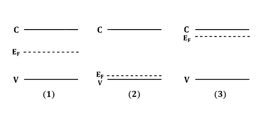
The band diagrams of three semiconductors p, n and intrinsic are given in the figures (1), (2) and (3). C and V are the conduction and valence bands and E F E_F E F
(a) intrinsic, n and p (b) p, intrinsic and n (c) intrinsic, p and n (d) n, intrinsic and p Show answer and solution
Answer: (b)
Intrinsic: E F E_F E F E F E_F E F E F E_F E F Figure (2): E F E_F E F Figure (1): E F E_F E F E F E_F E F So (2), (1), (3) are p, intrinsic and n: the answer is (b). Report a mistake Q35 MHT CET 2025 · 23 APR · SHIFT 1 Easy ☆
Intrinsic & Extrinsic Semiconductors · n-type & p-type doping
Which of the following statements is TRUE for n-type semiconductor?
(a) Holes are majority carriers and trivalent atoms are dopants. (b) Electrons are majority carriers and trivalent atoms are dopants. (c) Holes are minority carriers and pentavalent atoms are dopants. (d) Electrons are minority carriers and pentavalent atoms are dopants. Show answer and solution
Answer: (c)
n-type: pentavalent dopant gives extra electrons, so electrons are majority carriers. Holes are then minority carriers. So the answer is (c). Report a mistake Q36 MHT CET 2025 · 22 APR · SHIFT 2 Easy ☆
Intrinsic & Extrinsic Semiconductors · n-type & p-type doping
In n-type semiconductor, free electrons donated by the impurity atoms occupy energy levels in
(a) the conduction band. (b) the valence band. (c) the band gap and are close to the conduction band. (d) the band gap and are close to the valence band. Show answer and solution
Answer: (c)
The donor electron of a pentavalent impurity is loosely bound. Its level lies in the band gap, just below the conduction band. So the answer is (c). Report a mistake Q37 MHT CET 2025 · 22 APR · SHIFT 1 Easy ☆
Intrinsic & Extrinsic Semiconductors · Mass action law
In a pure silicon crystal electron-hole concentration is 1 0 16 10^{16} 1 0 16 m 3 \text{m}^{3} m 3 1 0 21 10^{21} 1 0 21 m 3 \text{m}^{3} m 3
(a) 1 0 5 10^{5} 1 0 5 (b) 1 0 11 10^{11} 1 0 11 (c) 1 0 19 10^{19} 1 0 19 (d) 1 0 21 10^{21} 1 0 21 Show answer and solution
Answer: (b)
Phosphorus is a donor, so n e ≈ 1 0 21 m − 3 n_e \approx 10^{21}\ \text{m}^{-3} n e ≈ 1 0 21 m − 3 n h = n i 2 n e = 1 0 32 1 0 21 = 1 0 11 m − 3 n_h = \dfrac{n_i^2}{n_e} = \dfrac{10^{32}}{10^{21}} = 10^{11}\ \text{m}^{-3} n h = n e n i 2 = 1 0 21 1 0 32 = 1 0 11 m − 3 So the answer is (b) 1 0 11 10^{11} 1 0 11 Report a mistake Q38 MHT CET 2025 · 25 APR · SHIFT 2 Easy ☆
Intrinsic & Extrinsic Semiconductors · Effect of temperature
A piece of semiconductor is connected in series in an electric circuit. On increasing the temperature, the current in the circuit will
(a) decrease. (b) remain unchanged. (c) increase. (d) stop flowing. Show answer and solution
Answer: (c)
Raising T T T More carriers lowers the resistance of the semiconductor, so I = V / R I = V/R I = V / R So the answer is (c) increase. Report a mistake Q39 MHT CET 2025 · 23 APR · SHIFT 2 Easy ☆
Intrinsic & Extrinsic Semiconductors · Effect of temperature
By increasing the temperature, the specific resistance of a conductor and a semiconductor respectively
(a) increases, increases. (b) decreases, decreases. (c) increases, decreases. (d) decreases, increases. Show answer and solution
Answer: (c)
Conductor: carrier number is fixed, but more lattice vibrations increase collisions, so ρ \rho ρ Semiconductor: carrier number rises sharply with T T T ρ \rho ρ So the answer is (c) increases, decreases. Report a mistake Q40 MHT CET 2025 · 21 APR · SHIFT 1 Easy ☆
Intrinsic & Extrinsic Semiconductors · Effect of temperature
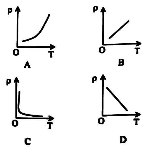
Which graph shows correctly the temperature (T). dependence of resistivity ( ρ ) (\rho) ( ρ )
Show answer and solution
Answer: (a)
For a semiconductor, carrier density rises roughly exponentially with T T T ρ \rho ρ Graph C shows this falling, curved (decaying) shape; A and B rise (metal-like) and D is a straight line. So the answer is (a) C. Report a mistake Q41 JEE Main 2025 · 4 APR · SHIFT 2 Medium ☆
Intrinsic & Extrinsic Semiconductors · n-type & p-type doping
Consider a n-type semiconductor in which n e n_e n e n h n_h n h
(A) Holes are minority carriers
(B) The dopant is a pentavalent atom
(C) n e n h ≠ n i 2 n_e n_h \neq n_i^2 n e n h = n i 2
(where n i n_i n i n e n h ⩾ n i 2 n_e n_h \geqslant n_i^2 n e n h ⩾ n i 2
(E) The holes are not generated due to the donors
Choose the correct answer from the options given below:
(a) (A), (B), (E) only (b) (A), (C), (E) only (c) (A), (B), (C) only (d) (A), (C), (D) only Show answer and solution
Answer: (a)
(A) In n-type, holes are minority carriers: true. (B) The dopant is pentavalent: true. (C) Mass action law gives n e n h = n i 2 n_e n_h = n_i^2 n e n h = n i 2 n e n h ≠ n i 2 n_e n_h \neq n_i^2 n e n h = n i 2 (E) Donors release only electrons; holes come from thermal pair generation: true. So the answer is (a) (A), (B), (E) only. Report a mistake Q42 MHT CET 2024 · 16 MAY · SHIFT 2 Easy ☆
Intrinsic & Extrinsic Semiconductors · n-type & p-type doping
When a small amount of impurity atoms are added to semiconductor, then generally its resistivity
(a) may increase or decrease depending upon the percentage of doping. (b) increases. (c) decreases. (d) does not change. Show answer and solution
Answer: (c)
Doping greatly increases the number of charge carriers. So conductivity rises and resistivity decreases. So the answer is (c) decreases. Report a mistake Q43 MHT CET 2024 · 15 MAY · SHIFT 1 Easy ☆
Intrinsic & Extrinsic Semiconductors · n-type & p-type doping
In an extrinsic n-type semiconductor, the free electrons donated by the impurity atoms occupy energy levels in
(a) the conduction band. (b) the valance band. (c) the band gap and are close to conduction band. (d) the band gap and are close to valance band. Show answer and solution
Answer: (c)
Donor electrons of a pentavalent impurity occupy the donor level. The donor level lies in the band gap, close to the conduction band (about 0.01 0.01 0.01 0.05 eV 0.05\text{ eV} 0.05 eV So the answer is (c). Report a mistake Q44 MHT CET 2024 · 3 MAY · SHIFT 2 Easy ☆
Intrinsic & Extrinsic Semiconductors · n-type & p-type doping
Which one of the following statements is true? A p-type semiconductor is doped with
(a) trivalent impurity and electrons are majority carriers. (b) pentavalent impurity and electrons are minority carriers. (c) pentavalent impurity and holes are minority carriers. (d) trivalent impurity and holes are majority carriers. Show answer and solution
Answer: (d)
p-type: trivalent dopant (B, Al, Ga, In) creates a hole for each atom. So holes are majority carriers and electrons minority carriers. So the answer is (d). Report a mistake Q45 MHT CET 2024 · 11 MAY · SHIFT 1 Easy ☆
Intrinsic & Extrinsic Semiconductors · Mass action law
If ' n e n_e n e n h n_h n h
(a) n e ≫ n h n_e \gg n_h n e ≫ n h (b) n e ≪ n h n_e \ll n_h n e ≪ n h (c) n e ⩽ n h n_e \leqslant n_h n e ⩽ n h (d) n e = n h n_e = n_h n e = n h Show answer and solution
Answer: (a)
Phosphorus is pentavalent, so heavy doping gives a strongly n-type material. Since n e n h = n i 2 n_e n_h = n_i^2 n e n h = n i 2 n e n_e n e n h n_h n h So the answer is (a) n e ≫ n h n_e \gg n_h n e ≫ n h Report a mistake Q46 JEE Main 2024 · 6 APR · SHIFT 2 Medium ☆
Intrinsic & Extrinsic Semiconductors · n-type & p-type doping
The acceptor level of a p-type semiconductor is 6 eV 6\text{ eV} 6 eV h c = 1242 eV nm hc = 1242\text{ eV nm} h c = 1242 eV nm
(a) 407 nm (b) 103.5 nm (c) 414 nm (d) 207 nm Show answer and solution
Answer: (d)
To create a hole, a photon must lift a valence electron to the acceptor level: E = h c λ ≥ 6 E = \dfrac{hc}{\lambda} \ge 6 E = λ h c ≥ 6 λ m a x = h c E = 1242 6 \lambda_{max} = \dfrac{hc}{E} = \dfrac{1242}{6} λ ma x = E h c = 6 1242 λ m a x = 207 \lambda_{max} = 207 λ ma x = 207 So the answer is (d) 207 nm. Report a mistake Q47 JEE Main 2024 · 1 FEB · SHIFT 2 Difficult ☆
Intrinsic & Extrinsic Semiconductors · Effect of temperature
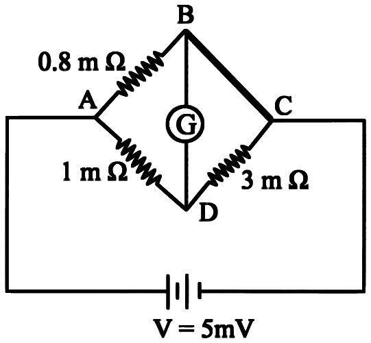
To measure the temperature coefficient of resistivity α \alpha α 2 5 ∘ C 25^\circ\text{C} 2 5 ∘ C 3 m Ω 3\text{ m}\Omega 3 m Ω BC \text{BC} BC 2 ∘ C/s 2^\circ\text{C/s} 2 ∘ C/s G \text{G} G 10 s 10\text{ s} 10 s α \alpha α
(a) − 1 × 1 0 − 2 ∘ C − 1 -1 \times 10^{-2}\ {}^\circ\text{C}^{-1} − 1 × 1 0 − 2 ∘ C − 1 (b) − 2 × 1 0 − 2 ∘ C − 1 -2 \times 10^{-2}\ {}^\circ\text{C}^{-1} − 2 × 1 0 − 2 ∘ C − 1 (c) − 2.5 × 1 0 − 2 ∘ C − 1 -2.5 \times 10^{-2}\ {}^\circ\text{C}^{-1} − 2.5 × 1 0 − 2 ∘ C − 1 (d) − 1.5 × 1 0 − 2 ∘ C − 1 -1.5 \times 10^{-2}\ {}^\circ\text{C}^{-1} − 1.5 × 1 0 − 2 ∘ C − 1 Show answer and solution
Answer: (a)
At balance (no deflection): R A B R B C = R A D R D C ⇒ 0.8 R B C = 1 3 \dfrac{R_{AB}}{R_{BC}} = \dfrac{R_{AD}}{R_{DC}} \Rightarrow \dfrac{0.8}{R_{BC}} = \dfrac{1}{3} R BC R A B = R D C R A D ⇒ R BC 0.8 = 3 1 R B C = 2.4 m Ω R_{BC} = 2.4\ \text{m}\Omega R BC = 2.4 m Ω Temperature change in 10 s: Δ T = − 2 × 10 = − 20 ∘ C \Delta T = -2 \times 10 = -20\ ^\circ\text{C} Δ T = − 2 × 10 = − 20 ∘ C R = R 0 ( 1 + α Δ T ) ⇒ 2.4 = 3 ( 1 − 20 α ) ⇒ ∣ α ∣ = 0.6 3 × 20 = 1 × 1 0 − 2 ∘ C − 1 R = R_0(1 + \alpha\,\Delta T) \Rightarrow 2.4 = 3(1 - 20\alpha) \Rightarrow |\alpha| = \dfrac{0.6}{3 \times 20} = 1 \times 10^{-2}\ ^\circ\text{C}^{-1} R = R 0 ( 1 + α Δ T ) ⇒ 2.4 = 3 ( 1 − 20 α ) ⇒ ∣ α ∣ = 3 × 20 0.6 = 1 × 1 0 − 2 ∘ C − 1 A semiconductor has a negative temperature coefficient. So the answer is (a) − 1 × 1 0 − 2 ∘ C − 1 -1 \times 10^{-2}\ ^\circ\text{C}^{-1} − 1 × 1 0 − 2 ∘ C − 1 Report a mistake Q48 MHT CET 2023 · 14 MAY · SHIFT 2 Easy ☆
Intrinsic & Extrinsic Semiconductors · Intrinsic semiconductors
When the conductivity of a semiconductor is only due to the breaking of the covalent bonds, the semiconductor is called
(a) donor (b) intrinsic (c) acceptor (d) extrinsic Show answer and solution
Answer: (b)
Carriers produced only by breaking covalent bonds means a pure semiconductor with no dopant. This is an intrinsic semiconductor. So the answer is (b) intrinsic. Report a mistake Q49 MHT CET 2023 · 9 MAY · SHIFT 1 Easy ☆
Intrinsic & Extrinsic Semiconductors · Intrinsic semiconductors
For an intrinsic semiconductor ( n h (n_h ( n h n e n_e n e
(a) n h < n e n_h < n_e n h < n e (b) n h = n e n_h = n_e n h = n e (c) n h = n e 2 n_h = \frac{n_e}{2} n h = 2 n e (d) n h > n e n_h > n_e n h > n e Show answer and solution
Answer: (b)
In an intrinsic semiconductor electrons and holes are created in pairs. So n h = n e n_h = n_e n h = n e So the answer is (b). Report a mistake Q50 MHT CET 2023 · 13 MAY · SHIFT 2 Easy ☆
Intrinsic & Extrinsic Semiconductors · n-type & p-type doping
Doping of a semiconductor (with small impurity atoms) generally changes the resistivity as follows.
(a) Decreases (b) Does not change (c) May increase or decrease depending on the dopant (d) Increase Show answer and solution
Answer: (a)
Doping adds many extra charge carriers to the semiconductor. More carriers mean higher conductivity, so resistivity decreases. So the answer is (a) Decreases. Report a mistake Q51 NEET 2023 Easy ☆
Intrinsic & Extrinsic Semiconductors · n-type & p-type doping
A p-type extrinsic semiconductor is obtained when Germanium is doped with:
(a) Antimony (b) Phosphorous (c) Arsenic (d) Boron Show answer and solution
Answer: (d)
A p-type semiconductor needs a trivalent (acceptor) impurity. Sb, P and As are pentavalent; boron is trivalent. So the answer is (d) Boron. Report a mistake Q52 JEE Main 2023 · 6 APR · SHIFT 1 Easy ☆
Intrinsic & Extrinsic Semiconductors · Effect of temperature
The resistivity ( ρ ) (\rho) ( ρ )
Show answer and solution
Answer: (d)
Semiconductor resistivity falls with temperature because the number of carriers rises roughly as e − E g / 2 k T e^{-E_g/2kT} e − E g /2 k T So ρ \rho ρ T T T Graphs (a) and (c) rise with T T T So the answer is (d). Report a mistake Q53 JEE Main 2023 · 31 JAN · SHIFT 1 Easy ☆
Intrinsic & Extrinsic Semiconductors · Effect of temperature
The effect of increase in temperature on the number of electrons in conduction band (n e n_e n e
(a) n e n_e n e (b) Both n e n_e n e (c) n e n_e n e (d) Both n e n_e n e Show answer and solution
Answer: (c)
Higher T T T n e n_e n e More carriers means lower resistance. So the answer is (c) n e n_e n e Report a mistake Q54 JEE Main 2023 · 1 FEB · SHIFT 1 Medium ☆
Intrinsic & Extrinsic Semiconductors · n-type & p-type doping
Match List I with List II:
Choose the correct answer from the options given below:
List I List II A. Intrinsic semiconductor I. Fermi-level near the valence band B. n-type semiconductor II. Fermi-level in the middle of valence and conduction band. C. p-type semiconductor III. Fermi-level near the conduction band D. Metals IV. Fermi-level inside the conduction band
(a) A-III, B-I, C-II, D-IV (b) A-II, B-I, C-III, D-IV (c) A-I, B-II, C-III, D-IV (d) A-II, B-III, C-I, D-IV Show answer and solution
Answer: (d)
Intrinsic: equal n e n_e n e n h n_h n h E F E_F E F n-type: excess electrons push E F E_F E F p-type: excess holes pull E F E_F E F E F E_F E F So the answer is (d) A-II, B-III, C-I, D-IV. Report a mistake Q55 MHT CET 2023 · 10 MAY · SHIFT 2 Medium ☆
Intrinsic & Extrinsic Semiconductors · Mass action law
A pure Si \text{Si} Si 4 × 1 0 28 4 \times 10^{28} 4 × 1 0 28 m 3 \text{m}^{3} m 3
(a) 4 × 1 0 34 m − 3 4 \times 10^{34}\text{ m}^{-3} 4 × 1 0 34 m − 3 (b) 4 × 1 0 28 m − 3 4 \times 10^{28}\text{ m}^{-3} 4 × 1 0 28 m − 3 (c) 4 × 1 0 22 m − 3 4 \times 10^{22}\text{ m}^{-3} 4 × 1 0 22 m − 3 (d) 4 × 1 0 20 m − 3 4 \times 10^{20}\text{ m}^{-3} 4 × 1 0 20 m − 3 Show answer and solution
Answer: (c)
Each Sb (pentavalent) atom donates one free electron, so n e ≈ N D n_e \approx N_D n e ≈ N D 1 ppm means 1 dopant atom per 1 0 6 10^{6} 1 0 6 N D = 4 × 1 0 28 1 0 6 = 4 × 1 0 22 m − 3 N_D = \dfrac{4 \times 10^{28}}{10^{6}} = 4 \times 10^{22}\ \text{m}^{-3} N D = 1 0 6 4 × 1 0 28 = 4 × 1 0 22 m − 3 So the answer is (c) 4 × 1 0 22 m − 3 4 \times 10^{22}\ \text{m}^{-3} 4 × 1 0 22 m − 3 Report a mistake Q56 NEET 2022 · PHASE 1 Easy ☆
Intrinsic & Extrinsic Semiconductors · Effect of temperature
As the temperature increases, the electrical resistance
(a) Increases for both conductors and semiconductors (b) Decreases for both conductors and semiconductors (c) Increases for conductors but decreases for semiconductors (d) Decreases for conductors but increases for semiconductors Show answer and solution
Answer: (c)
Conductors: more lattice vibration at higher T T T R R R Semiconductors: more carriers are generated at higher T T T R R R So the answer is (c). Report a mistake Q57 JEE Main 2021 · 26 AUG · SHIFT 1 Easy ☆
Intrinsic & Extrinsic Semiconductors · n-type & p-type doping
Statement I: By doping silicon semiconductor with pentavalent material, the electrons density increases.
Statement II: The n-type semiconductor has net negative charge.
In the light of the above statements, choose the most appropriate answer from the options given below:
(a) Statement - I is true but Statement - II is false. (b) Statement - I is false but Statement - II is true. (c) Both Statement I and Statement II are true. (d) Both Statement I and Statement II are false. Show answer and solution
Answer: (a)
Statement I: pentavalent donors add free electrons, so electron density increases: true. Statement II: each donor that gives an electron becomes a fixed positive ion, so the crystal stays electrically neutral: false. So the answer is (a). Report a mistake Q58 MHT CET 2021 · 21 SEP · SHIFT 1 Easy ☆
Intrinsic & Extrinsic Semiconductors · Mass action law
In a pure silicon, number of electrons and holes per unit volume are 1.6 × 1 0 16 m − 3 1.6 \times 10^{16}\text{ m}^{-3} 1.6 × 1 0 16 m − 3 4 × 1 0 22 m − 3 4 \times 10^{22}\text{ m}^{-3} 4 × 1 0 22 m − 3
(a) 6.4 × 1 0 − 9 m − 3 6.4 \times 10^{-9}\text{ m}^{-3} 6.4 × 1 0 − 9 m − 3 (b) 6.4 × 1 0 9 m − 3 6.4 \times 10^{9}\text{ m}^{-3} 6.4 × 1 0 9 m − 3 (c) 6.4 × 1 0 − 10 m − 3 6.4 \times 10^{-10}\text{ m}^{-3} 6.4 × 1 0 − 10 m − 3 (d) 6.4 × 1 0 10 m − 3 6.4 \times 10^{10}\text{ m}^{-3} 6.4 × 1 0 10 m − 3 Show answer and solution
Answer: (b)
Mass action law: n e = n i 2 n h n_e = \dfrac{n_i^2}{n_h} n e = n h n i 2 n e = ( 1.6 × 1 0 16 ) 2 4 × 1 0 22 = 2.56 × 1 0 32 4 × 1 0 22 n_e = \dfrac{(1.6\times10^{16})^2}{4\times10^{22}} = \dfrac{2.56\times10^{32}}{4\times10^{22}} n e = 4 × 1 0 22 ( 1.6 × 1 0 16 ) 2 = 4 × 1 0 22 2.56 × 1 0 32 n e = 6.4 × 1 0 9 m − 3 n_e = 6.4\times10^{9}\ \text{m}^{-3} n e = 6.4 × 1 0 9 m − 3 So the answer is (b). Report a mistake Q59 JEE Main 2021 · 25 JUL · SHIFT 2 Easy ☆
Intrinsic & Extrinsic Semiconductors · Mass action law
In a semiconductor, the number density of intrinsic charge carries at 27∘ ^\circ ∘ × \times × × \times × × \times ×
Numerical answer type. Work it out, then open the answer.
Show answer and solution
Answer: 5
Mass action law: n e n h = n i 2 n_e n_h = n_i^2 n e n h = n i 2 n e = ( 1.5 × 1 0 16 ) 2 4.5 × 1 0 22 = 2.25 × 1 0 32 4.5 × 1 0 22 n_e = \dfrac{(1.5\times10^{16})^2}{4.5\times10^{22}} = \dfrac{2.25\times10^{32}}{4.5\times10^{22}} n e = 4.5 × 1 0 22 ( 1.5 × 1 0 16 ) 2 = 4.5 × 1 0 22 2.25 × 1 0 32 n e = 5 × 1 0 9 / m 3 n_e = 5\times10^{9}\ /\text{m}^3 n e = 5 × 1 0 9 / m 3 So the answer is 5. Report a mistake Q60 MHT CET 2021 · 23 SEP · SHIFT 2 Easy ☆
Intrinsic & Extrinsic Semiconductors · Effect of temperature
When the temperature of a semiconductor is increased, its resistance and electric conductivity respectively.
(a) increases and decreases (b) decreases and decreases (c) increases and increases (d) decreases and increases Show answer and solution
Answer: (d)
Higher T T T So resistance decreases and conductivity σ = e ( n e μ e + n h μ h ) \sigma = e(n_e\mu_e + n_h\mu_h) σ = e ( n e μ e + n h μ h ) So the answer is (d) decreases and increases. Report a mistake Q61 JEE Main 2021 · 25 FEB · SHIFT 2 Medium ☆
Intrinsic & Extrinsic Semiconductors · n-type & p-type doping
For extrinsic semiconductors; when doping level is increased;
(a) Fermi-level of both p-type and n-type semiconductors will go upward for T > TFK and downward for T < TFK, where TF is Fermi temperature. (b) Fermi-level of p-type semiconductor will go upward and Fermi-level of n-type semiconductors will go downward (c) Fermi-level of p and n-type semiconductors will not be affected. (d) Fermi-level of p-type semiconductors will go downward and Fermi-level of n-type semiconductor will go upward. Show answer and solution
Answer: (d)
More donor doping in n-type adds electrons, so E F E_F E F More acceptor doping in p-type adds holes, so E F E_F E F So the answer is (d). Report a mistake Q62 NEET 2021 Medium ☆
Intrinsic & Extrinsic Semiconductors · Conductivity & mobility
The electron concentration in an n-type semiconductor is the same as hole concentration in a p-type semiconductor. An external field (electric) is applied across each of them. Compare the currents in them.
(a) No current will flow in p-type, current will only flow in n-type (b) Current in n-type = current in p-type (c) current in p-type > current in n-type (d) current in n-type > current in p-type Show answer and solution
Answer: (d)
Current I = n e A v d = n e A μ E I = neAv_d = neA\mu E I = n e A v d = n e A μ E I ∝ μ I \propto \mu I ∝ μ Electrons are more mobile than holes: μ e > μ h \mu_e > \mu_h μ e > μ h So the answer is (d) current in n-type > current in p-type. Report a mistake Q63 MHT CET 2021 · 20 SEP · SHIFT 1 Medium ☆
Intrinsic & Extrinsic Semiconductors · Effect of temperature
Silicon and copper are cooled from 300 K to 100 K, the specific resistance (resistivity)
(a) increases in both copper and silicon (b) decreases in both copper and silicon (c) decreases in copper and increases in silicon (d) increases in copper and decreases in silicon Show answer and solution
Answer: (c)
Copper (metal): on cooling, lattice vibrations reduce, collisions fall, so resistivity decreases. Silicon (semiconductor): on cooling, fewer electrons cross the band gap, carrier number falls, so resistivity increases. So the answer is (c) decreases in copper and increases in silicon. Report a mistake Q64 MHT CET 2020 · 19 OCT · SHIFT 2 Easy ☆
Intrinsic & Extrinsic Semiconductors · Intrinsic semiconductors
In an intrinsic semiconductor, at an ordinary temperature, the correct relation between the number of electrons per unit volume n e n_e n e n h n_h n h
(a) n e = n h n_e = n_h n e = n h (b) n e > n h n_e > n_h n e > n h (c) n e < n h n_e < n_h n e < n h (d) n e = n h = 0 n_e = n_h = 0 n e = n h = 0 Show answer and solution
Answer: (a)
Thermal breaking of each covalent bond creates one electron and one hole. So n e = n h n_e = n_h n e = n h So the answer is (a) n e = n h n_e = n_h n e = n h Report a mistake Q65 MHT CET 2020 · 16 OCT · SHIFT 1 Easy ☆
Intrinsic & Extrinsic Semiconductors · n-type & p-type doping
When a small amount of impurity atoms are added to a semiconductor, then generally its resistivity
(a) may increase or decrease depending upon the percentage of doping (b) increases (c) decreases (d) does not change Show answer and solution
Answer: (c)
Doping adds extra charge carriers (electrons from donors or holes from acceptors). More carriers means higher conductivity σ = e ( n e μ e + n h μ h ) \sigma = e(n_e\mu_e + n_h\mu_h) σ = e ( n e μ e + n h μ h ) ρ = 1 / σ \rho = 1/\sigma ρ = 1/ σ So the answer is (c) decreases. Report a mistake Q66 NEET 2020 · PHASE 2 Easy ☆
Intrinsic & Extrinsic Semiconductors · n-type & p-type doping
An intrinsic semiconductor is converted into n n n
(a) Germanium (b) Phosphorous (c) Aluminium (d) Silver Show answer and solution
Answer: (b)
An n-type semiconductor needs a pentavalent (donor) impurity. Phosphorus has 5 valence electrons; Al is trivalent, Ge is tetravalent, Ag is a metal. So the answer is (b) Phosphorous. Report a mistake Q67 MHT CET 2020 · 16 OCT · SHIFT 2 Easy ☆
Intrinsic & Extrinsic Semiconductors · Effect of temperature
At absolute zero temperature, pure silicon behaves as
(a) non-metal (b) insulator (c) metal (d) extrinsic semiconductor Show answer and solution
Answer: (b)
At 0 0 0 ≈ 1.1 \approx 1.1 ≈ 1.1 The conduction band is empty and the valence band full, so there are no free carriers. So the answer is (b) insulator. Report a mistake Q68 NEET 2019 Easy ☆
Intrinsic & Extrinsic Semiconductors · n-type & p-type doping
For a p-type semiconductor, which of the following statements is true?
(a) Holes are the majority carriers and trivalent atoms are the dopants. (b) Holes are the majority carriers and pentavalent atoms are the dopants. (c) Electrons are the majority carriers and pentavalent atoms are the dopants (d) Electrons are the majority carriers and trivalent atoms are the dopants. Show answer and solution
Answer: (a)
p-type is made by adding trivalent (acceptor) atoms such as B, Al, In. Each acceptor creates a hole, so holes are the majority carriers. So the answer is (a). Report a mistake Q69 JEE Main 2019 · 9 JAN · SHIFT 1 Medium ☆
Intrinsic & Extrinsic Semiconductors · Conductivity & mobility
Mobility of electrons in a semiconductor is defined as the ratio of their drift velocity to the applied electric field. If, for an n-type semiconductor, the density of electrons is 1019 m− 3 {}^{-3} − 3
(a) 2 Ω 2\ \Omega 2 Ω (b) 4 Ω \Omega Ω (c) 0.4 Ω \Omega Ω (d) 0.2 Ω \Omega Ω Show answer and solution
Answer: (c)
For an n-type semiconductor, σ = n e μ e \sigma = n e \mu_e σ = n e μ e ρ = 1 n e μ e \rho = \dfrac{1}{n e \mu_e} ρ = n e μ e 1 ρ = 1 1 0 19 × 1.6 × 1 0 − 19 × 1.6 = 1 2.56 \rho = \dfrac{1}{10^{19} \times 1.6 \times 10^{-19} \times 1.6} = \dfrac{1}{2.56} ρ = 1 0 19 × 1.6 × 1 0 − 19 × 1.6 1 = 2.56 1 ρ ≈ 0.39 Ω m \rho \approx 0.39\ \Omega\,\text{m} ρ ≈ 0.39 Ω m So the answer is (c) 0.4 Ω m 0.4\ \Omega\,\text{m} 0.4 Ω m Report a mistake Q70 JEE Main 2017 · 8 APR · SHIFT 1 Medium ☆
Intrinsic & Extrinsic Semiconductors · Conductivity & mobility
What is the conductivity of a semiconductor sample having electron concentration of 5 × 1 0 18 m − 3 , 5 \times 10^{18}\text{ m}^{-3}, 5 × 1 0 18 m − 3 , 5 × 1 0 19 m − 3 , 5 \times 10^{19}\text{ m}^{-3}, 5 × 1 0 19 m − 3 , − 1 {}^{-1} − 1 − 1 {}^{-1} − 1 − 1 {}^{-1} − 1
(Take charge of electron as 1.6 × \times × − - −
(a) 1.68 (Ω \Omega Ω − 1 {}^{-1} − 1 (b) 1.83 (Ω \Omega Ω − 1 {}^{-1} − 1 (c) 0.59 (Ω \Omega Ω − 1 {}^{-1} − 1 (d) 1.20 (Ω \Omega Ω − 1 {}^{-1} − 1 Show answer and solution
Answer: (a)
σ = e ( n e μ e + n h μ h ) \sigma = e(n_e \mu_e + n_h \mu_h) σ = e ( n e μ e + n h μ h ) n e μ e = 5 × 1 0 18 × 2.0 = 1.0 × 1 0 19 n_e \mu_e = 5 \times 10^{18} \times 2.0 = 1.0 \times 10^{19} n e μ e = 5 × 1 0 18 × 2.0 = 1.0 × 1 0 19 n h μ h = 5 × 1 0 19 × 0.01 = 0.05 × 1 0 19 n_h \mu_h = 5 \times 10^{19} \times 0.01 = 0.05 \times 10^{19} n h μ h = 5 × 1 0 19 × 0.01 = 0.05 × 1 0 19 σ = 1.6 × 1 0 − 19 × 1.05 × 1 0 19 = 1.68 ( Ω -m ) − 1 \sigma = 1.6 \times 10^{-19} \times 1.05 \times 10^{19} = 1.68\ (\Omega\text{-m})^{-1} σ = 1.6 × 1 0 − 19 × 1.05 × 1 0 19 = 1.68 ( Ω -m ) − 1 So the answer is (a) 1.68 ( Ω -m ) − 1 1.68\ (\Omega\text{-m})^{-1} 1.68 ( Ω -m ) − 1 Report a mistake Q71 JEE Main 2016 Difficult ☆
Intrinsic & Extrinsic Semiconductors · Effect of temperature
The temperature dependence of resistance of Cu \text{Cu} Cu Si \text{Si} Si 300 − 400 K , 300 - 400\text{ K}, 300 − 400 K ,
(a) Linear increases for Cu , \text{Cu}, Cu , Si . \text{Si}. Si . (b) Linear decrease for Cu , \text{Cu}, Cu , Si \text{Si} Si (c) Linear increase for Cu , \text{Cu}, Cu , Si . \text{Si}. Si . (d) Linear increase for Cu , \text{Cu}, Cu , Si \text{Si} Si Show answer and solution
Answer: (a)
Cu (metal): R = R 0 ( 1 + α Δ T ) R = R_0(1 + \alpha \Delta T) R = R 0 ( 1 + α Δ T ) Undoped Si: carrier density ∝ e − E g / 2 k T \propto e^{-E_g/2kT} ∝ e − E g /2 k T So the answer is (a) linear increase for Cu, exponential decrease for Si. Report a mistake Q72 NEET 2013 Easy ☆
Intrinsic & Extrinsic Semiconductors · n-type & p-type doping
In a n-type semiconductor, which of the following statements is true?
(a) Holes are minority carriers and pentavalent atoms are dopants. (b) Holes are majority carriers and trivalent atoms are dopants. (c) Electrons are majority carriers and trivalent atoms are dopants. (d) Electrons are minority carriers and pentavalent atoms are dopants. Show answer and solution
Answer: (a)
n-type is made by adding pentavalent (donor) atoms such as P, As, Sb. Donors give free electrons, so electrons are majority and holes are minority carriers. So the answer is (a). Report a mistake Q73 NEET 2011 · AIPMT · PRELIMS Easy ☆
Intrinsic & Extrinsic Semiconductors · n-type & p-type doping
If a small amount of antimony is added to germanium crystal
(a) it becomes a p-type semiconductor (b) the antimony becomes an acceptor atom (c) there will be more free electrons than holes in the semiconductor (d) its resistance is increased Show answer and solution
Answer: (c)
Antimony is pentavalent, so it acts as a donor in Ge. Ge becomes n-type: free electrons outnumber holes, and resistance decreases. So the answer is (c). Report a mistake Q74 NEET 2011 · AIPMT · MAINS Easy ☆
Intrinsic & Extrinsic Semiconductors · Mass action law
Pure Si at 500 K has equal number of electron (ne) and hole (nh) concentrations of 1.5 × \times × − 3 {}^{-3} − 3 × \times × − 3 {}^{-3} − 3
(a) p-type having electron concentration ne = 5 × \times × − 3 {}^{-3} − 3 (b) n-type with electron concentration ne = 5 × \times × − 3 {}^{-3} − 3 (c) p-type with electron concentration ne = 2.5 × \times × − 3 {}^{-3} − 3 (d) n-type with electron concentration ne = 2.5 × \times × − 3 {}^{-3} − 3 Show answer and solution
Answer: (a)
Indium is trivalent, so the doped Si is p-type. n e = n i 2 n h = ( 1.5 × 1 0 16 ) 2 4.5 × 1 0 22 = 2.25 × 1 0 32 4.5 × 1 0 22 n_e = \dfrac{n_i^2}{n_h} = \dfrac{(1.5\times10^{16})^2}{4.5\times10^{22}} = \dfrac{2.25\times10^{32}}{4.5\times10^{22}} n e = n h n i 2 = 4.5 × 1 0 22 ( 1.5 × 1 0 16 ) 2 = 4.5 × 1 0 22 2.25 × 1 0 32 n e = 5 × 1 0 9 m − 3 n_e = 5\times10^{9}\ \text{m}^{-3} n e = 5 × 1 0 9 m − 3 So the answer is (a) p-type with n e = 5 × 1 0 9 m − 3 n_e = 5\times10^9\ \text{m}^{-3} n e = 5 × 1 0 9 m − 3 Report a mistake Q75 NEET 2010 · AIPMT · PRELIMS Easy ☆
Intrinsic & Extrinsic Semiconductors · n-type & p-type doping
Which one of the following statement is false?
(a) Pure Si doped with trivalent impurities gives a p-type semiconductor. (b) Majority carries in a n-type semiconductor are holes. (c) Minority carries in a p-type semiconductor are electrons. (d) The resistance of intrinisic semiconductor decreases with increase of temperature. Show answer and solution
Answer: (b)
(a) Trivalent doping gives p-type: true. (b) In n-type the majority carriers are electrons, not holes: false. (c) Minority carriers in p-type are electrons: true. (d) Intrinsic resistance falls as T T T So the false statement is (b). Report a mistake Q76 NEET 2007 · AIPMT Medium ☆
Intrinsic & Extrinsic Semiconductors · n-type & p-type doping
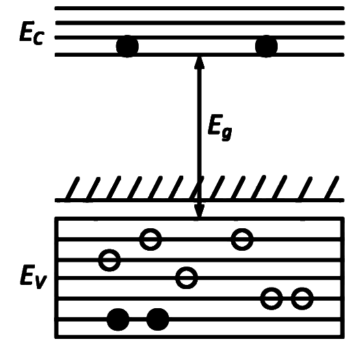
In the energy band diagram of a material shown below, the open circles and filled circles denote holes and electrons respectively. The material is
(a) an insulator (b) a metal (c) an n-type semiconductor (d) a p-type semiconductor. Show answer and solution
Answer: (d)
The diagram shows a band gap E g E_g E g E C E_C E C E V E_V E V Holes (open circles) in the valence band outnumber electrons (filled circles) in the conduction band. Holes are the majority carriers, so the material is p-type. So the answer is (d) a p-type semiconductor. Report a mistake Q77 JEE Main 2006 · AIEEE Medium ☆
Intrinsic & Extrinsic Semiconductors · Conductivity & mobility
If the ratio of the concentration of electrons to that of holes in a semiconductor is 7 5 \frac{7}{5} 5 7 7 4 , \frac{7}{4}, 4 7 ,
(a) 5 8 \frac{5}{8} 8 5 (b) 4 5 \frac{4}{5} 5 4 (c) 5 4 \frac{5}{4} 4 5 (d) 4 7 \frac{4}{7} 7 4 Show answer and solution
Answer: (c)
I = n e A v d ⇒ v d ∝ I n I = neAv_d \Rightarrow v_d \propto \dfrac{I}{n} I = n e A v d ⇒ v d ∝ n I v e v h = I e I h × n h n e = 7 4 × 5 7 = 5 4 \dfrac{v_e}{v_h} = \dfrac{I_e}{I_h} \times \dfrac{n_h}{n_e} = \dfrac{7}{4} \times \dfrac{5}{7} = \dfrac{5}{4} v h v e = I h I e × n e n h = 4 7 × 7 5 = 4 5 So the answer is (c) 5 4 \dfrac{5}{4} 4 5 Report a mistake Q78 JEE Main 2004 · AIEEE Easy ☆
Intrinsic & Extrinsic Semiconductors · Effect of temperature
A piece of copper and another of germanium are cooled from room temperature to 77 K , 77\text{ K}, 77 K ,
(a) copper increases and germanium decreases (b) each of them decreases (c) each of them increases (d) copper decreases and germanium increases Show answer and solution
Answer: (d)
Copper (metal): fewer lattice vibrations on cooling, so resistance decreases. Germanium (semiconductor): fewer free carriers on cooling, so resistance increases. So the answer is (d). Report a mistake Q79 JEE Main 2003 · AIEEE Easy ☆
Intrinsic & Extrinsic Semiconductors · Effect of temperature
A strip of copper and another of germanium are cooled from room temperature to 80 K . 80\text{ K}. 80 K .
(a) each of these decreases (b) copper strip increases and that of germanium decreases (c) copper strip decreases and that of germanium increases (d) each of these increases Show answer and solution
Answer: (c)
Copper (metal): cooling reduces collisions with the vibrating lattice, so resistance decreases. Germanium (semiconductor): cooling reduces carrier generation, so resistance increases. So the answer is (c). Report a mistake Q80 JEE Main 2003 · AIEEE Medium ☆
Intrinsic & Extrinsic Semiconductors · Effect of temperature
The difference in the variation of resistance with temperature in a metal and a semiconductor arises essentially due to the difference in the
(a) crystal structure (b) variation of the number of charge carriers with temperature (c) type of bonding (d) variation of scattering mechanism with temperature Show answer and solution
Answer: (b)
In a metal the number of free electrons is fixed; rising temperature only increases scattering, so R R R In a semiconductor the number of carriers rises sharply with temperature, so R R R So the answer is (b) variation of the number of charge carriers with temperature. Report a mistake Q81 JEE Main 2002 · AIEEE Easy ☆
Intrinsic & Extrinsic Semiconductors · Effect of temperature
At absolute zero, Si acts as
(a) non-metal (b) metal (c) insulator (d) none of these Show answer and solution
Answer: (c)
At absolute zero no electron in Si can cross the band gap. Conduction band empty, valence band full: no free charge carriers. So the answer is (c) insulator. Report a mistake Q82 JEE Main 2002 · AIEEE Easy ☆
Intrinsic & Extrinsic Semiconductors · Effect of temperature
By increasing the temperature, the specific resistance of a conductor and a semiconductor
(a) increases for both (b) decreases for both (c) increases, decreases (d) decreases, increases Show answer and solution
Answer: (c)
Conductor: more lattice vibration at higher T T T Semiconductor: more electron-hole pairs at higher T T T So the answer is (c) increases, decreases. Report a mistake Q83 NEET 1999 · AIPMT Easy ☆
Intrinsic & Extrinsic Semiconductors · n-type & p-type doping
Which of the following when added as an impurity into silicon produces n n n
Show answer and solution
Answer: (a)
n-type silicon needs a pentavalent donor. P (group 15) is pentavalent; Al and B are trivalent, Mg is divalent. So the answer is (a) P. Report a mistake Q84 NEET 1999 · AIPMT Easy ☆
Intrinsic & Extrinsic Semiconductors · n-type & p-type doping
In a junction diode, the holes are due to
(a) protons (b) extra electrons (c) neutrons (d) missing electrons Show answer and solution
Answer: (d)
A hole is a vacancy left in a covalent bond when an electron is absent. It behaves like a positive charge + e +e + e So the answer is (d) missing electrons. Report a mistake Q85 NEET 1999 · AIPMT Easy ☆
Intrinsic & Extrinsic Semiconductors · n-type & p-type doping
In p p p
(a) holes (b) electrons (c) protons (d) neutrons Show answer and solution
Answer: (a)
p-type is doped with trivalent acceptors, each creating a hole. So holes far outnumber free electrons. So the answer is (a) holes. Report a mistake Q86 NEET 1997 · AIPMT Easy ☆
Intrinsic & Extrinsic Semiconductors · n-type & p-type doping
To obtain a p-type germanium semiconductor, it must be doped with
(a) indium (b) phosphorus (c) arsenic (d) antimony Show answer and solution
Answer: (a)
p-type Ge needs a trivalent acceptor. Indium is trivalent; P, As and Sb are pentavalent. So the answer is (a) indium. Report a mistake Q87 NEET 1996 · AIPMT Easy ☆
Intrinsic & Extrinsic Semiconductors · n-type & p-type doping
When arsenic is added as an impurity to silicon, the resulting material is
(a) n-type conductor (b) n-type semiconductor (c) p-type semiconductor (d) none of these Show answer and solution
Answer: (b)
Arsenic is pentavalent, so it donates a free electron in Si. Electrons become majority carriers, but the material is still a semiconductor. So the answer is (b) n-type semiconductor. Report a mistake Q88 NEET 1992 · AIPMT Easy ☆
Intrinsic & Extrinsic Semiconductors · Effect of temperature
A piece of copper and other of germanium are cooled from the room temperature to 80 K 80\text{ K} 80 K
(a) resistance of each will increase (b) resistance of copper will decrease (c) the resistance of copper will increase while that of germanium will decrease (d) the resistance of copper will decrease while that of germanium will increase Show answer and solution
Answer: (d)
Copper is a metal: cooling reduces lattice vibrations, so its resistance decreases. Germanium is a semiconductor: cooling reduces the number of free carriers, so its resistance increases. So the answer is (d). Report a mistake Q89 NEET 1989 · AIPMT Medium ☆
Intrinsic & Extrinsic Semiconductors · Effect of temperature
When n type semiconductor is heated
(a) number of electrons increases while that of holes decreases (b) number of holes increases while that of electrons decreases (c) number of electrons and holes remain same (d) number of electrons and holes increases equally Show answer and solution
Answer: (d)
Heating breaks covalent bonds and creates electron-hole pairs. Each broken bond adds one free electron and one hole, so both increase by the same number. So the answer is (d) number of electrons and holes increases equally. Report a mistake Q90 NEET 1988 · AIPMT Easy ☆
Intrinsic & Extrinsic Semiconductors · Effect of temperature
At absolute zero, Si acts as
(a) non metal (b) metal (c) insulator (d) none of these Show answer and solution
Answer: (c)
At 0 0 0 No free carriers exist, so Si cannot conduct. So the answer is (c) insulator. Report a mistake Q91 MHT CET 2026 · 14 MAY · SHIFT 1 Easy ☆
P-N Junction Diode · Depletion layer & barrier
In the middle of the depletion region of reversed biased p-n junction the
(a) electric field is zero (b) potential is infinite (c) electric field is maximum (d) potential is zero Show answer and solution
Answer: (c)
The depletion region has fixed positive ions on the n-side and negative ions on the p-side. The field points from n to p and is strongest at the junction (middle of the depletion region); reverse bias makes it even larger. So the answer is (c) electric field is maximum. Report a mistake Q92 MHT CET 2026 · 20 APR · SHIFT 2 Easy ☆
P-N Junction Diode · Depletion layer & barrier
The depletion region of p-n junction
(a) increases if reverse biased. (b) increases if forward biased. (c) decreases if reverse biased. (d) remains same in reverse and forward biasing. Show answer and solution
Answer: (a)
Reverse bias pulls majority carriers away from the junction, exposing more fixed ions. Forward bias pushes carriers toward the junction and narrows it. So the answer is (a) increases if reverse biased. Report a mistake Q93 MHT CET 2026 · 13 MAY · SHIFT 2 Easy ☆
P-N Junction Diode · Forward & reverse bias
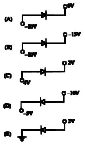
The forward biased diode connection is
Show answer and solution
Answer: (a)
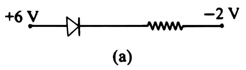
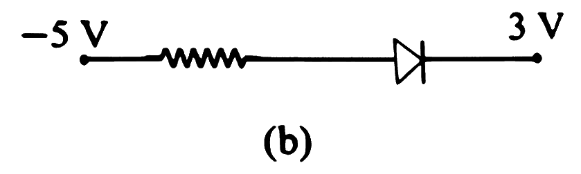
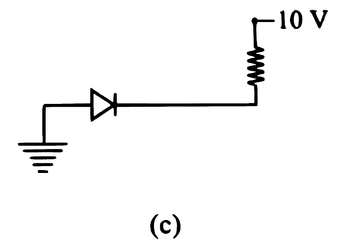
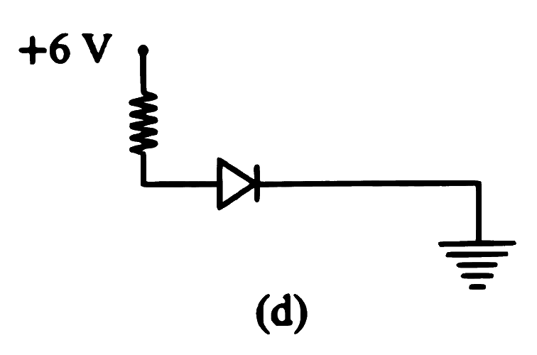
Forward bias: the p-side (arrow end, anode) is at a higher potential than the n-side (bar end, cathode). (a) anode + 2 V +2\ \text{V} + 2 V − 2 V -2\ \text{V} − 2 V 2 V < 4 V 2\ \text{V} < 4\ \text{V} 2 V < 4 V (c) − 3 V = − 3 V -3\ \text{V} = -3\ \text{V} − 3 V = − 3 V − 2 V < + 2 V -2\ \text{V} < +2\ \text{V} − 2 V < + 2 V So the answer is (a). Report a mistake Q94 MHT CET 2026 · 18 APR · SHIFT 1 Easy ☆
P-N Junction Diode · Forward & reverse bias
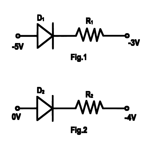
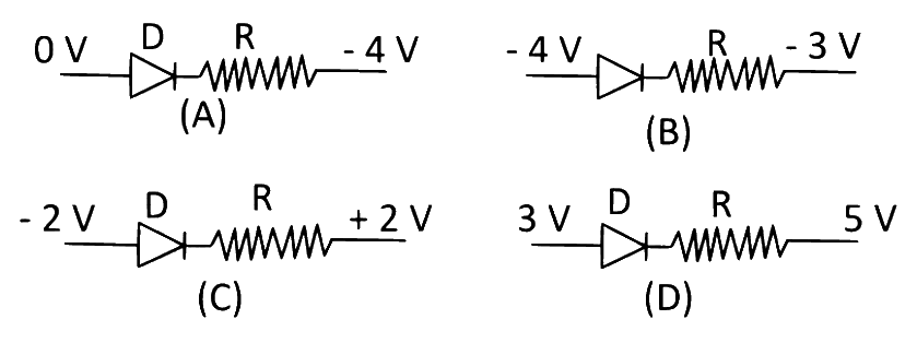
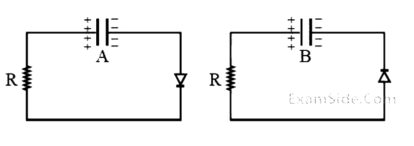
A diode and resistance are connected as shown in figures.
Out of the following statements, which one is true?
Diode in
A) fig (1) and fig (2) are both forward biased.
B) fig (1) and fig (2) are both reverse biased.
C) fig (1) is forward biased and in fig (2) is reverse biased.
D) fig (1) is reverse biased and in fig (2) is forward biased.
Show answer and solution
Answer: (a)
Forward bias needs anode potential > cathode-side potential. Fig. 1: anode − 5 V -5\ \text{V} − 5 V − 3 V -3\ \text{V} − 3 V − 5 < − 3 -5 < -3 − 5 < − 3 Fig. 2: anode 0 V 0\ \text{V} 0 V − 4 V -4\ \text{V} − 4 V 0 > − 4 0 > -4 0 > − 4 Statement D is true, so the answer is (a) D. Report a mistake Q95 MHT CET 2026 · 15 APR · SHIFT 1 Easy ☆
P-N Junction Diode · Forward & reverse bias
For a p-n junction diode, breakdown voltage occurs when
(a) reverse bias is decreased (b) reverse bias is not changed (c) reverse-bias is increased (d) forward bias is increased Show answer and solution
Answer: (c)
In reverse bias only a tiny saturation current flows. When the reverse voltage is increased to the breakdown value, the current rises sharply (Zener or avalanche breakdown). So the answer is (c) reverse bias is increased. Report a mistake Q96 MHT CET 2026 · 15 APR · SHIFT 1 Easy ☆
P-N Junction Diode · Forward & reverse bias
If p-n junction diode is forward biased then
(a) width of depletion layer decreases. (b) width of depletion layer increases. (c) barrier voltage increases (d) electric conduction is not possible Show answer and solution
Answer: (a)
Forward bias opposes the barrier field and pushes majority carriers toward the junction. So the barrier voltage falls, the depletion layer narrows and current flows. So the answer is (a) width of depletion layer decreases. Report a mistake Q97 NEET 2026 Easy ☆
P-N Junction Diode · Forward & reverse bias
Two statements are given below:
A. When the forward bias voltage across a p-n junction diode increases above a certain threshold voltage, the diode current increases significantly.
B. This current is called reverse saturation current.
Choose the correct answer from the options given below:
(a) Both Statements A and B are true (b) Statement A is true, but Statement B is false (c) Both Statements A A A B B B (d) Statement A is false, but Statement B is true Show answer and solution
Answer: (b)
A: above the threshold (knee) voltage the forward current rises sharply. True. B: this is forward current carried by majority carriers; reverse saturation current is the tiny current in reverse bias. False. So the answer is (b) Statement A is true, but Statement B is false. Report a mistake Q98 JEE Main 2026 · 5 APR · SHIFT 2 Medium ☆
P-N Junction Diode · Depletion layer & barrier
In a semiconductor p p p p p p n n n 1 0 15 10^{15} 1 0 15 / cm 3 /\text{cm}^{3} / cm 3 1 0 18 10^{18} 1 0 18 / cm 3 /\text{cm}^{3} / cm 3
(a) Widths of depletion region on either side of the interface are equal (b) The depletion region width is more on p -side compared to that in n -side (c) The depletion region width is more on n n n p p p (d) No depletion region forms because of unequal doping concentrations on p and n -sides Show answer and solution
Answer: (b)
Charge neutrality of the depletion layer: N A x p = N D x n N_A x_p = N_D x_n N A x p = N D x n x p x n = N D N A = 1 0 18 1 0 15 = 1 0 3 \dfrac{x_p}{x_n} = \dfrac{N_D}{N_A} = \dfrac{10^{18}}{10^{15}} = 10^{3} x n x p = N A N D = 1 0 15 1 0 18 = 1 0 3 The lightly doped p side has the wider depletion region. So the answer is (b). Report a mistake Q99 MHT CET 2026 · 17 APR · SHIFT 2 Medium ☆
P-N Junction Diode · Forward & reverse bias
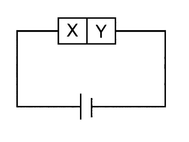
A semiconductor X is made by doping a germanium crystal with indium ( Z = 49 ) (Z = 49) ( Z = 49 ) ( Z = 33 ) (Z = 33) ( Z = 33 )
(a) X is p-type, Y is n-type and the junction is forward biased. (b) X is p-type, Y is n-type and the junction is reverse biased. (c) X is n-type, Y is p-type and the junction is forward biased. (d) X is n-type, Y is p-type and the junction is reverse biased. Show answer and solution
Answer: (a)
Indium (group 13, trivalent) makes Ge p-type, so X is p-type; Arsenic (group 15, pentavalent) makes Ge n-type, so Y is n-type. In the figure the longer (positive) plate of the battery is on the left, connected to X. Positive terminal to p side means forward bias. So the answer is (a). Report a mistake Q100 NEET 2026 · RE-NEET Medium ☆
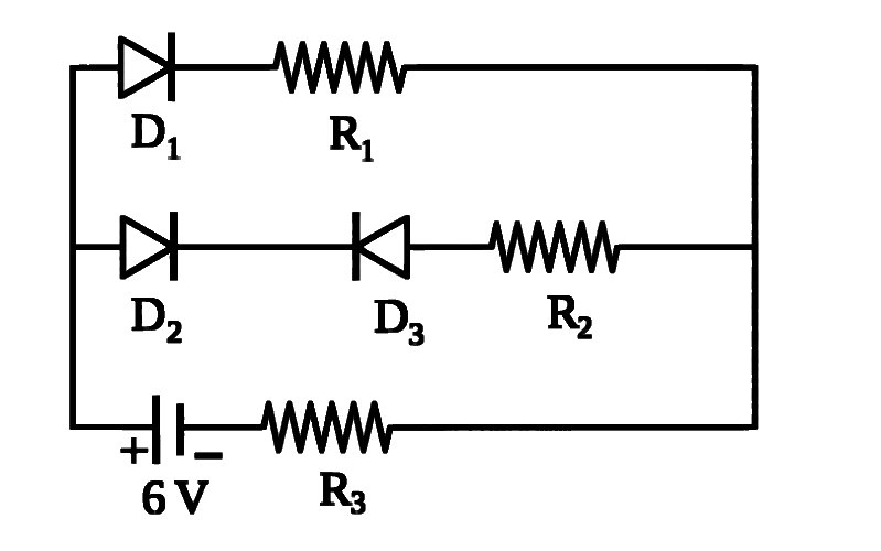
P-N Junction Diode · Forward & reverse bias
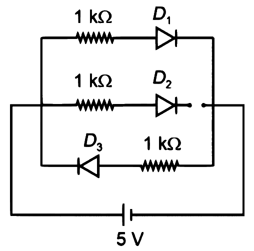
Three identical p-n junction diodes D 1 , D 2 D_1, D_2 D 1 , D 2 D 3 D_3 D 3 D 1 , D 2 D_1, D_2 D 1 , D 2 D 3 D_3 D 3 W 1 , W 2 W_1, W_2 W 1 , W 2 W 3 W_3 W 3
(a) W 2 > W 1 = W 3 W_2 > W_1 = W_3 W 2 > W 1 = W 3 (b) W 1 > W 2 > W 3 W_1 > W_2 > W_3 W 1 > W 2 > W 3 (c) W 3 = W 1 > W 2 W_3 = W_1 > W_2 W 3 = W 1 > W 2 (d) W 3 > W 2 > W 1 W_3 > W_2 > W_1 W 3 > W 2 > W 1 Show answer and solution
Answer: (d)
Battery positive terminal (long plate) is on the left node, negative on the right node. D 1 D_1 D 1 D 3 D_3 D 3 D 2 D_2 D 2 D 2 D_2 D 2 So W 3 > W 2 > W 1 W_3 > W_2 > W_1 W 3 > W 2 > W 1 Report a mistake Q101 JEE Main 2026 · 4 APR · SHIFT 2 Medium ☆
P-N Junction Diode · Forward & reverse bias
Given below are two statements: one is labelled as Assertion A and the other is labelled as Reason R \mathbf{R} R
Assertion A: A diode under reverse-biased condition provides very small current which is nearly independent of voltage until a critical limit at which the current increases drastically. Reason R: Below the critical voltage limit, only majority charge carriers flow which increases drastically above critical voltage.
choose the correct answer from the options given below
(a) Both A \mathbf{A} A R \mathbf{R} R R \mathbf{R} R A \mathbf{A} A (b) Both A \mathbf{A} A R \mathbf{R} R R \mathbf{R} R A \mathbf{A} A (c) A is true but R \mathbf{R} R (d) A is false but R \mathbf{R} R Show answer and solution
Answer: (c)
Assertion: reverse current is small and almost constant up to the breakdown voltage, then rises sharply. True. Reason: below breakdown the reverse current is due to minority carriers, not majority carriers. False. So the answer is (c) A is true but R is false. Report a mistake Q102 MHT CET 2026 · 12 MAY · SHIFT 2 Medium ☆
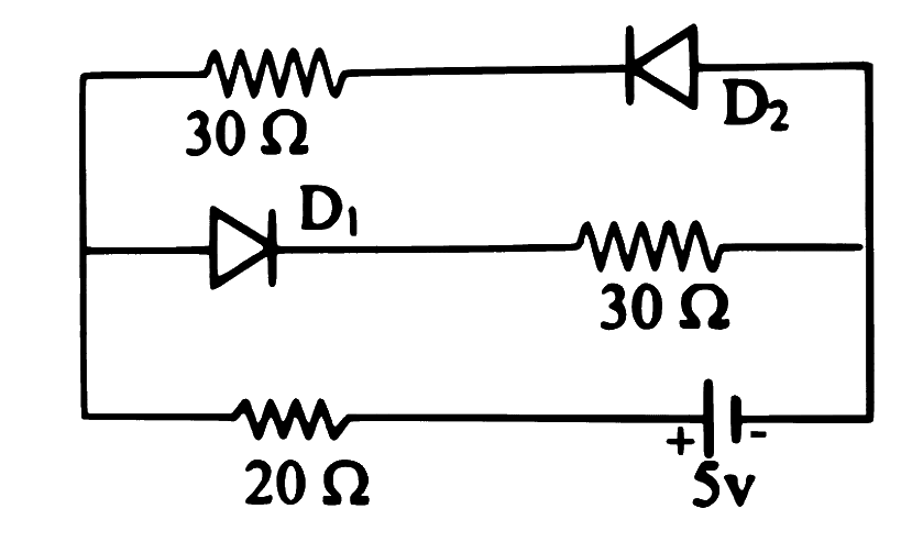
P-N Junction Diode · Diode circuits
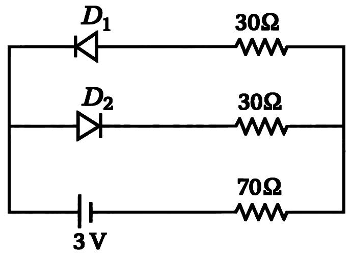
The circuit shown contains two ideal diodes D 1 D_1 D 1 D 2 D_2 D 2 3 3 3 70 Ω 70\ \Omega 70 Ω
(a) 0.01 0.01 0.01 (b) 0.02 0.02 0.02 (c) 0.03 0.03 0.03 (d) 0 0 0 Show answer and solution
Answer: (c)
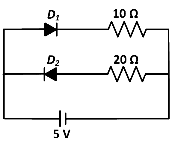
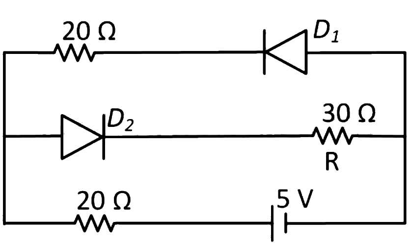
The left plate of the cell is positive, so current reaches the left junction and moves right through the diode branches. D 1 D_1 D 1 D 2 D_2 D 2 Circuit: 30 Ω 30\ \Omega 30 Ω D 2 D_2 D 2 70 Ω 70\ \Omega 70 Ω I = 3 30 + 70 = 0.03 I = \dfrac{3}{30 + 70} = 0.03 I = 30 + 70 3 = 0.03 So the answer is (c) 0.03 0.03 0.03 Report a mistake Q103 MHT CET 2026 · 12 MAY · SHIFT 1 Medium ☆
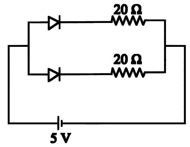
P-N Junction Diode · Diode circuits
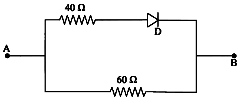
In one branch, 40 Ω 40\ \Omega 40 Ω 40 Ω 40\ \Omega 40 Ω
(a) 40 Ω 40\ \Omega 40 Ω 20 Ω 20\ \Omega 20 Ω (b) 60 Ω 60\ \Omega 60 Ω 30 Ω 30\ \Omega 30 Ω (c) 20 Ω 20\ \Omega 20 Ω 40 Ω 40\ \Omega 40 Ω (d) 30 Ω 30\ \Omega 30 Ω 60 Ω 60\ \Omega 60 Ω Show answer and solution
Answer: (c)
Forward biased ideal diode acts as a short: both 40 Ω 40\ \Omega 40 Ω R = 40 × 40 80 = 20 Ω R = \dfrac{40\times 40}{80} = 20\ \Omega R = 80 40 × 40 = 20 Ω Reverse biased ideal diode acts as an open switch: only one 40 Ω 40\ \Omega 40 Ω R = 40 Ω R = 40\ \Omega R = 40 Ω So the answer is (c) 20 Ω 20\ \Omega 20 Ω 40 Ω 40\ \Omega 40 Ω Report a mistake Q104 MHT CET 2026 · 19 APR · SHIFT 2 Medium ☆
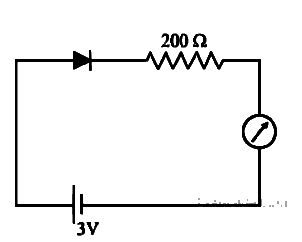
P-N Junction Diode · Diode circuits
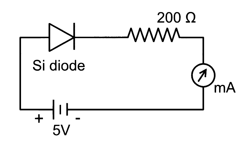
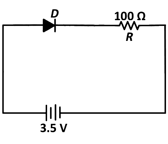
In the following electrical circuit, the reading in the milliammeter is
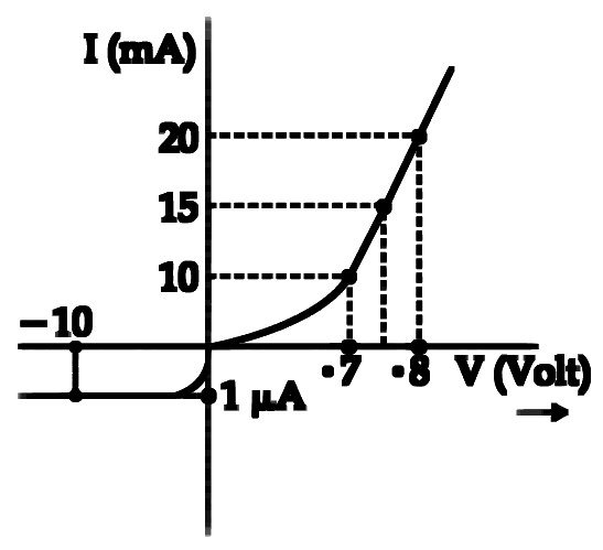
(Take knee voltage of silicon diode = 0.7 = 0.7 = 0.7
(a) 25.5 25.5 25.5 (b) 21.5 21.5 21.5 (c) 18.5 18.5 18.5 (d) 15.8 15.8 15.8 Show answer and solution
Answer: (b)
The diode's p-side is at the battery's positive terminal, so it is forward biased with a 0.7 0.7 0.7 I = V − V k R = 5 − 0.7 200 I = \dfrac{V - V_k}{R} = \dfrac{5 - 0.7}{200} I = R V − V k = 200 5 − 0.7 I = 4.3 200 = 0.0215 I = \dfrac{4.3}{200} = 0.0215 I = 200 4.3 = 0.0215 = 21.5 = 21.5 = 21.5 So the answer is (b) 21.5 21.5 21.5 Report a mistake Q105 MHT CET 2026 · 17 APR · SHIFT 1 Medium ☆
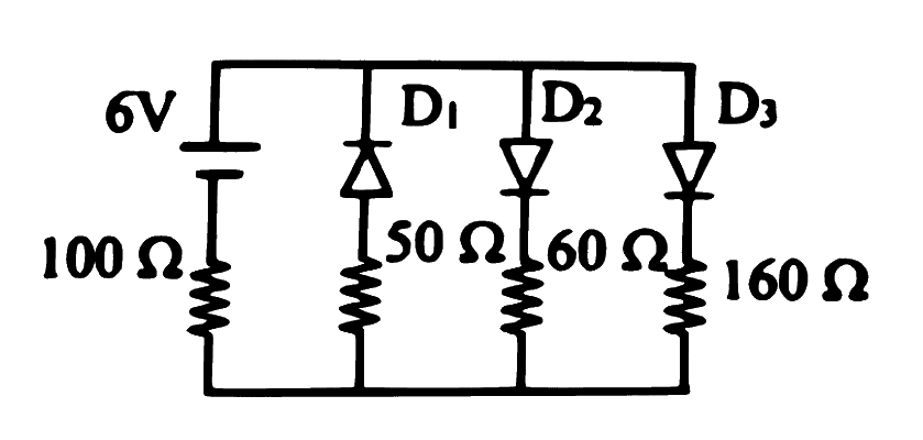
P-N Junction Diode · Diode circuits
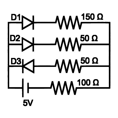
In the circuit shown in figure all the three diodes D1, D2, D3 have forward resistance 50 Ω 50\ \Omega 50 Ω 100 Ω 100\ \Omega 100 Ω
(a) 60 60 60 (b) 30 30 30 (c) 20 20 20 (d) 10 10 10 Show answer and solution
Answer: (b)
The left terminal of the battery is positive. D 1 D_1 D 1 D 2 D_2 D 2 D 3 D_3 D 3 Branch resistances: D 1 D_1 D 1 = 50 + 150 = 200 Ω = 50 + 150 = 200\ \Omega = 50 + 150 = 200 Ω D 2 D_2 D 2 = 50 + 50 = 100 Ω = 50 + 50 = 100\ \Omega = 50 + 50 = 100 Ω Parallel: 200 × 100 300 = 200 3 Ω \dfrac{200\times 100}{300} = \dfrac{200}{3}\ \Omega 300 200 × 100 = 3 200 Ω = 100 + 200 3 = 500 3 Ω = 100 + \dfrac{200}{3} = \dfrac{500}{3}\ \Omega = 100 + 3 200 = 3 500 Ω I = 5 500 / 3 = 0.03 I = \dfrac{5}{500/3} = 0.03 I = 500/3 5 = 0.03 = 30 = 30 = 30 100 Ω 100\ \Omega 100 Ω So the answer is (b) 30 30 30 Report a mistake Q106 MHT CET 2026 · 15 APR · SHIFT 2 Medium ☆
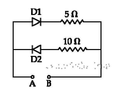
P-N Junction Diode · Diode circuits
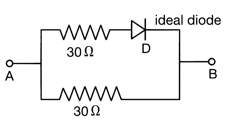
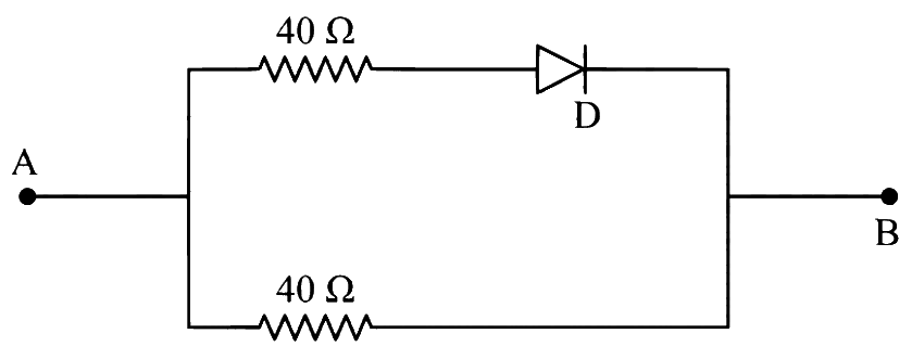
In the diagram shown, the resistance between points A and B is 'R 1 R_1 R 1 R 2 R_2 R 2 R 1 / R 2 R_1/R_2 R 1 / R 2
(a) 2 2 2 (b) 1 1 1 (c) 1 2 \frac{1}{2} 2 1 (d) 1 4 \frac{1}{4} 4 1 Show answer and solution
Answer: (c)
Forward bias: diode is a short, so the two 30 Ω 30\ \Omega 30 Ω R 1 = 15 Ω R_1 = 15\ \Omega R 1 = 15 Ω Reverse bias: diode branch is open, so only the lower 30 Ω 30\ \Omega 30 Ω R 2 = 30 Ω R_2 = 30\ \Omega R 2 = 30 Ω R 1 R 2 = 15 30 = 1 2 \dfrac{R_1}{R_2} = \dfrac{15}{30} = \dfrac{1}{2} R 2 R 1 = 30 15 = 2 1 So the answer is (c) 1 2 \frac{1}{2} 2 1 Report a mistake Q107 NEET 2026 Medium ☆
P-N Junction Diode · Diode circuits
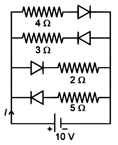
The current / in the circuit shown below is: (All diodes are ideal and identical)
(a) 5 3 A \frac{5}{3}\text{ A} 3 5 A (b) 5 9 A \frac{5}{9}\text{ A} 9 5 A (c) 1 3 A \frac{1}{3}\text{ A} 3 1 A (d) 15 2 A \frac{15}{2}\text{ A} 2 15 A Show answer and solution
Answer: (d)
The left terminal of the battery is positive, so current flows left to right through the branches. Diodes pointing right conduct: the 4 Ω 4\ \Omega 4 Ω 2 Ω 2\ \Omega 2 Ω 3 Ω 3\ \Omega 3 Ω 5 Ω 5\ \Omega 5 Ω R e q = 4 × 2 4 + 2 = 4 3 Ω R_{eq} = \dfrac{4\times 2}{4 + 2} = \dfrac{4}{3}\ \Omega R e q = 4 + 2 4 × 2 = 3 4 Ω I = 10 4 / 3 = 15 2 I = \dfrac{10}{4/3} = \dfrac{15}{2} I = 4/3 10 = 2 15 So the answer is (d) 15 2 \frac{15}{2} 2 15 Report a mistake Q108 JEE Main 2026 · 28 JAN · SHIFT 1 Medium ☆
P-N Junction Diode · Diode circuits
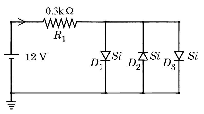
Assuming in forward bias condition there is a voltage drop of 0.7 V across a silicon diode, the current through diode D 1 D_1 D 1 ______ mA.
(Assume all diodes in the given circuit are identical)
(a) 17.6 (b) 18.8 (c) 20.15 (d) 11.7 Show answer and solution
Answer: (b)
D 1 D_1 D 1 D 3 D_3 D 3 D 2 D_2 D 2 The conducting diodes are in parallel, so the voltage across them is 0.7 0.7 0.7 Current through R 1 R_1 R 1 I = 12 − 0.7 300 = 11.3 300 = 37.67 I = \dfrac{12 - 0.7}{300} = \dfrac{11.3}{300} = 37.67 I = 300 12 − 0.7 = 300 11.3 = 37.67 Identical diodes share it equally: I D 1 = 37.67 2 ≈ 18.8 I_{D_1} = \dfrac{37.67}{2} \approx 18.8 I D 1 = 2 37.67 ≈ 18.8 So the answer is (b) 18.8 18.8 18.8 Report a mistake Q109 NEET 2026 Medium ☆
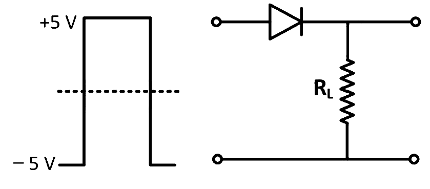
P-N Junction Diode · Waveforms & RC circuits
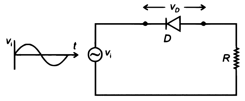
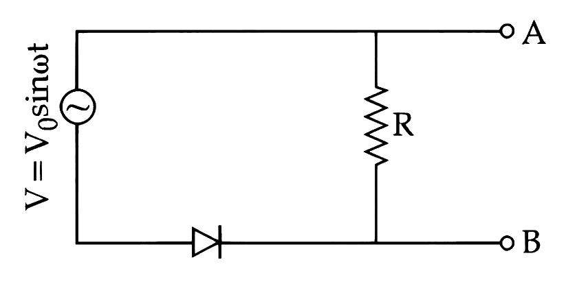
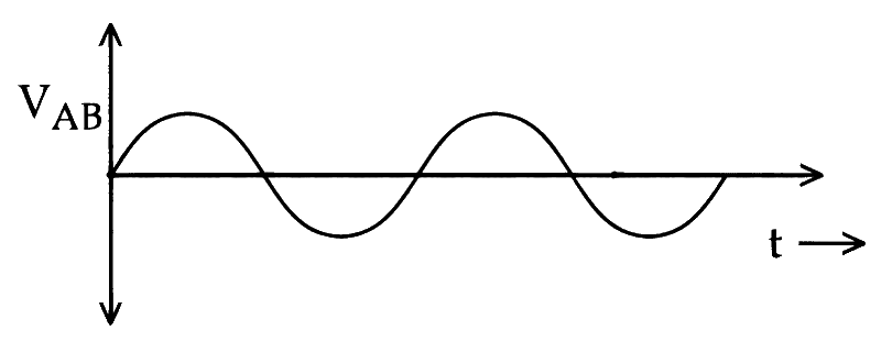
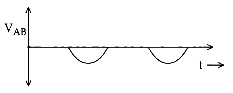
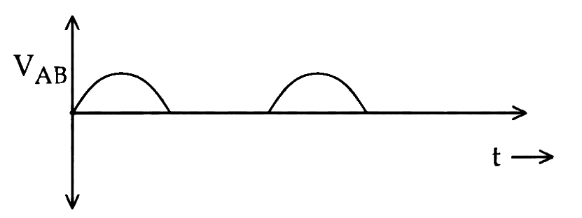
In the circuit shown below, the voltage appearing across the diode D will be of the form:
Show answer and solution
Answer: (d)
The diode's cathode faces the source's upper terminal and its anode faces R R R Positive half cycle: the diode is reverse biased, no current flows, so the whole input appears across it: v D = v i v_D = v_i v D = v i Negative half cycle: the diode is forward biased (ideal), so v D = 0 v_D = 0 v D = 0 v D v_D v D Report a mistake Q110 JEE Main 2026 · 21 JAN · SHIFT 2 Medium ☆
P-N Junction Diode · Waveforms & RC circuits
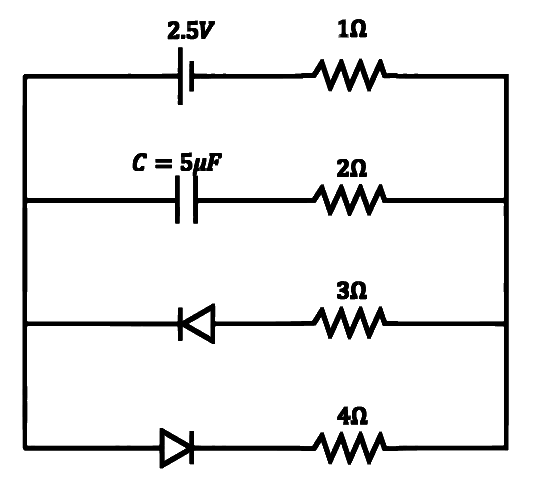
The charge stored by the capacitor C in the given circuit in the steady state is __________ µC.
Show answer and solution
Answer: (c)
In steady state no current flows in the capacitor branch. The battery makes the left node positive, so the 4 Ω 4\ \Omega 4 Ω 3 Ω 3\ \Omega 3 Ω Loop current: I = 2.5 1 + 4 = 0.5 I = \frac{2.5}{1 + 4} = 0.5 I = 1 + 4 2.5 = 0.5 Voltage between the two nodes = 2.5 − 0.5 × 1 = 2 = 2.5 - 0.5 \times 1 = 2 = 2.5 − 0.5 × 1 = 2 2 Ω 2\ \Omega 2 Ω Q = C V = 5 μ F × 2 = 10 μ C Q = CV = 5\ \mu\text{F} \times 2 = 10\ \mu\text{C} Q = C V = 5 μ F × 2 = 10 μ C Report a mistake Q111 JEE Main 2026 · 4 APR · SHIFT 1 Difficult ☆
P-N Junction Diode · Waveforms & RC circuits
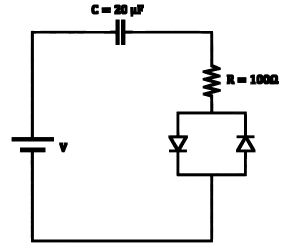
Consider a circuit consisting of a capacitor ( 20 μ F ) (20\,\mu\text{F}) ( 20 μ F ) ( 100 Ω ) (100\,\Omega) ( 100 Ω ) 10 Ω 10\,\Omega 10 Ω α × 1 0 − 3 s \alpha \times 10^{-3}\text{ s} α × 1 0 − 3 s α \alpha α ______
Show answer and solution
Answer: (a)
The two diodes are in parallel but opposite, so for either current direction exactly one is forward biased (10 Ω 10\ \Omega 10 Ω Total resistance in series with C C C R = 100 + 10 = 110 Ω R = 100 + 10 = 110\ \Omega R = 100 + 10 = 110 Ω τ = R C = 110 × 20 × 1 0 − 6 = 2.2 × 1 0 − 3 \tau = RC = 110 \times 20 \times 10^{-6} = 2.2 \times 10^{-3} τ = RC = 110 × 20 × 1 0 − 6 = 2.2 × 1 0 − 3 So α = 2.2 \alpha = 2.2 α = 2.2 Report a mistake Q112 JEE Main 2026 · 2 APR · SHIFT 1 Difficult ☆
P-N Junction Diode · Waveforms & RC circuits
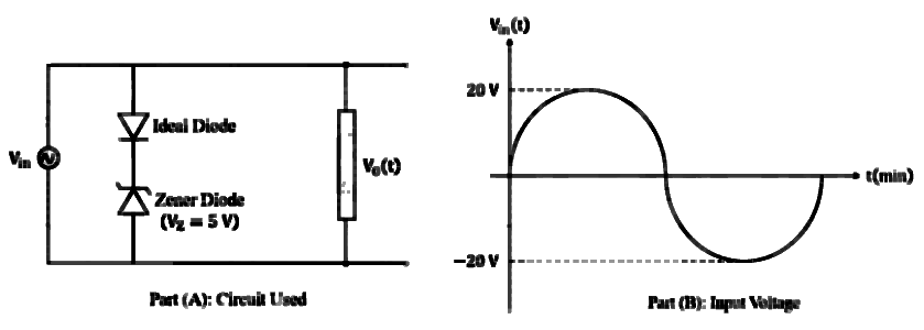
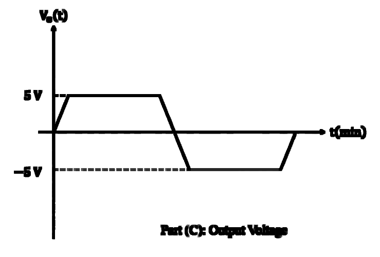
For the given circuit (shown in part (A)) the time dependent input voltage v i n ( t ) v_{in}(t) v in ( t ) v o ( t ) v_{o}(t) v o ( t )
Show answer and solution
Answer: (b)
The given branch (ideal diode + Zener, cathodes joined) conducts only when the top line is positive: diode forward, Zener in breakdown, so it clips the output at + 5 +5 + 5 For the negative half it is blocked, so another branch between X and Y is needed to clip at − 5 -5 − 5 This branch must be the same pair reversed: ideal diode and Zener joined anode to anode, with no resistor (a series resistor would stop the flat clipping). Then in the negative half the Zener breaks down at 5 V and the ideal diode conducts, giving v o = − 5 v_o = -5 v o = − 5 Report a mistake Q113 MHT CET 2025 · 19 APR · SHIFT 1 Easy ☆
P-N Junction Diode · Depletion layer & barrier
In the depletion layer of reverse biased p-n junction, the
(a) electric field is very small. (b) potential is maximum. (c) electric field is maximum. (d) potential is zero. Show answer and solution
Answer: (c)
The depletion layer contains only immobile ions, which set up a strong field from n to p. Reverse bias adds to this field, so the field in the depletion layer is maximum (largest at the junction). So the answer is (c) electric field is maximum. Report a mistake Q114 MHT CET 2025 · 5 MAY · SHIFT 2 Easy ☆
P-N Junction Diode · Forward & reverse bias
Which of the following figure represents forward bias diode?
Show answer and solution
Answer: (a)
Forward bias: anode (arrow side) potential > potential on the bar side. A: 0 > − 4 0 > -4 0 > − 4 − 4 < − 3 -4 < -3 − 4 < − 3 − 2 < + 2 -2 < +2 − 2 < + 2 3 < 5 3 < 5 3 < 5 So the answer is (a) A. Report a mistake Q115 MHT CET 2025 · 26 APR · SHIFT 2 Easy ☆
P-N Junction Diode · Forward & reverse bias
If p-n junction diode is forward biased, then
(a) electric conduction is not possible. (b) width of depletion layer decreases. (c) width of depletion layer increases. (d) barrier voltage increases. Show answer and solution
Answer: (b)
Forward bias reduces the barrier and pushes carriers into the depletion region. So the depletion layer becomes narrower and conduction takes place. So the answer is (b) width of depletion layer decreases. Report a mistake Q116 MHT CET 2025 · 26 APR · SHIFT 1 Easy ☆
P-N Junction Diode · Forward & reverse bias
Applying forward bias to p-n junction, the potential barrier
(a) increases. (b) decreases. (c) remains unchanged. (d) becomes zero. Show answer and solution
Answer: (b)
The applied forward voltage opposes the built-in barrier. Effective barrier becomes V B − V V_B - V V B − V So the answer is (b) decreases. Report a mistake Q117 MHT CET 2025 · 25 APR · SHIFT 1 Easy ☆
P-N Junction Diode · Forward & reverse bias
In which of the following figures, the p.n. junction diode is reverse biased?
Show answer and solution
Answer: (c)
Reverse bias: anode (arrow side) at a lower potential than the cathode (bar side). (a) anode + 6 V +6\ \text{V} + 6 V − 2 V -2\ \text{V} − 2 V + 6 V +6\ \text{V} + 6 V (b) anode at − 5 V -5\ \text{V} − 5 V 3 V 3\ \text{V} 3 V 10 V 10\ \text{V} 10 V Figure (b) is reverse biased, so the answer is (c) b. Report a mistake Q118 JEE Main 2025 · 22 JAN · SHIFT 1 Easy ☆
P-N Junction Diode · Forward & reverse bias
Which of the following circuits represents a forward biased diode?
Choose the correct answer from the options given below:
(a) (C) and (E) only (b) (A) and (D) only (c) (B), (D) and (E) only (d) (B), (C) and (E) only Show answer and solution
Answer: (d)
Forward bias: anode (triangle side) potential > > > (A) anode − 10 V -10\text{ V} − 10 V − 10 V -10\text{ V} − 10 V − 15 V -15\text{ V} − 15 V (C) anode 5 V 5\text{ V} 5 V 2 V 2\text{ V} 2 V (D) diode points left: cathode − 5 V -5\text{ V} − 5 V − 10 V -10\text{ V} − 10 V 0 V 0\text{ V} 0 V 2 V 2\text{ V} 2 V So the answer is (d) (B), (C) and (E) only. Report a mistake Q119 MHT CET 2025 · 20 APR · SHIFT 1 Easy ☆
P-N Junction Diode · Diode circuits
For an ideal diode, in forward and reverse biased condition the resistance is respectively
(a) infinite, zero. (b) infinite, infinite. (c) zero, zero. (d) zero, infinite. Show answer and solution
Answer: (d)
An ideal diode acts as a closed switch in forward bias: R f = 0 R_f = 0 R f = 0 It acts as an open switch in reverse bias: R r = ∞ R_r = \infty R r = ∞ So the answer is (d) zero, infinite. Report a mistake Q120 MHT CET 2025 · 19 APR · SHIFT 2 Medium ☆
P-N Junction Diode · Depletion layer & barrier
In unbiased p-n junction diode
(a) the potential is same everywhere. (b) there is an electric field at the junction directed from the p -type side to the n -type side. (c) there is an electric field at the junction directed from the n n n p p p (d) the p-type side is at higher potential than the n-type side. Show answer and solution
Answer: (c)
Electrons diffuse from n to p and holes from p to n, leaving + + + − - − So the n side is at a higher potential, and the field at the junction points from + + + − - − So the answer is (c). Report a mistake Q121 MHT CET 2025 · 21 APR · SHIFT 2 Medium ☆
P-N Junction Diode · Diode circuits
If the internal resistance of cell is negligible then current flowing through the circuit is
(a) 0.04 A 0.04\text{ A} 0.04 A (b) 0.06 A (c) 0.08 A (d) 0.10 A Show answer and solution
Answer: (d)
The battery's positive terminal sends current through 20 Ω 20\ \Omega 20 Ω D 1 D_1 D 1 30 Ω 30\ \Omega 30 Ω D 2 D_2 D 2 Total resistance = 20 + 30 = 50 Ω = 20 + 30 = 50\ \Omega = 20 + 30 = 50 Ω I = 5 50 = 0.1 I = \dfrac{5}{50} = 0.1 I = 50 5 = 0.1 So the answer is (d) 0.10 0.10 0.10 Report a mistake Q122 MHT CET 2025 · 20 APR · SHIFT 2 Medium ☆
P-N Junction Diode · Diode circuits
In the following circuit shown in figure, three diodes are connected each with forward resistance 40 Ω 40\ \Omega 40 Ω 100 Ω 100\ \Omega 100 Ω
(a) 18 mA (b) 36 mA (c) 9 mA (d) 27 mA Show answer and solution
Answer: (b)
The top rail is at the battery's positive terminal. D 1 D_1 D 1 D 2 D_2 D 2 D 3 D_3 D 3 Branches: D 2 D_2 D 2 40 + 60 = 100 Ω 40 + 60 = 100\ \Omega 40 + 60 = 100 Ω D 3 D_3 D 3 40 + 160 = 200 Ω 40 + 160 = 200\ \Omega 40 + 160 = 200 Ω = 100 × 200 300 = 200 3 Ω = \dfrac{100\times 200}{300} = \dfrac{200}{3}\ \Omega = 300 100 × 200 = 3 200 Ω Total = 100 + 200 3 = 500 3 Ω = 100 + \dfrac{200}{3} = \dfrac{500}{3}\ \Omega = 100 + 3 200 = 3 500 Ω I = 6 500 / 3 = 0.036 I = \dfrac{6}{500/3} = 0.036 I = 500/3 6 = 0.036 = 36 = 36 = 36 So the answer is (b) 36 36 36 Report a mistake Q123 JEE Main 2025 · 23 JAN · SHIFT 2 Medium ☆
P-N Junction Diode · Diode circuits
What is the current through the battery in the circuit shown below?
(a) 1.5 A (b) 0.25 A (c) 1.0 A (d) 0.5 A Show answer and solution
Answer: (d)
Both diodes point the same way and are forward biased, so both 20 Ω 20\ \Omega 20 Ω R e q = 20 × 20 40 = 10 Ω R_{eq} = \dfrac{20\times 20}{40} = 10\ \Omega R e q = 40 20 × 20 = 10 Ω I = 5 10 = 0.5 I = \dfrac{5}{10} = 0.5 I = 10 5 = 0.5 So the answer is (d) 0.5 0.5 0.5 Report a mistake Q124 JEE Main 2025 · 23 JAN · SHIFT 1 Medium ☆
P-N Junction Diode · Diode circuits
Refer to the circuit diagram given in the figure. which of the following observations are correct? A. Total resistance of circuit is 6 Ω 6\ \Omega 6 Ω
B. Current in Ammeter is 1 A
C. Potential across A B AB A B
D. Potential across CD is 4 Volts
E. Total resistance of the circuit is 8 Ω 8\ \Omega 8 Ω
Choose the correct answer from the options given below:
(a) B, C and E Only (b) A, C and D Only (c) A, B and C Only (d) A, B and D Only Show answer and solution
Answer: (d)
The diode points from D to A, so it is forward biased (short). Between D and B: 4 Ω ∥ 4 Ω = 2 Ω 4\ \Omega \parallel 4\ \Omega = 2\ \Omega 4 Ω ∥ 4 Ω = 2 Ω Total resistance = 4 + 2 = 6 Ω = 4 + 2 = 6\ \Omega = 4 + 2 = 6 Ω Ammeter current = 6 6 = 1 = \dfrac{6}{6} = 1 = 6 6 = 1 V C D = 1 × 4 = 4 V_{CD} = 1\times 4 = 4 V C D = 1 × 4 = 4 V A B = 0.5 × 4 = 2 V_{AB} = 0.5\times 4 = 2 V A B = 0.5 × 4 = 2 So the answer is (d) A, B and D only. Report a mistake Q125 JEE Main 2025 · 8 APR · SHIFT 2 Medium ☆
P-N Junction Diode · Waveforms & RC circuits
The output voltage in the following circuit is (Consider ideal diode case)
(a) 0 V (b) +5 V (c) −5 V (d) 10 V Show answer and solution
Answer: (a)
The output node is pulled toward + 5 +5 + 5 D 2 D_2 D 2 D 2 D_2 D 2 D 1 D_1 D 1 + 5 +5 + 5 V o u t = 0 V_{out} = 0 V o u t = 0 Report a mistake Q126 MHT CET 2024 · 4 MAY · SHIFT 2 Easy ☆
P-N Junction Diode · Depletion layer & barrier
The depletion layer in p-n junction region is caused by
(a) drift of electrons. (b) migration of impurity ions. (c) diffusion of charge carries. (d) drift of holes. Show answer and solution
Answer: (c)
Electrons diffuse from n to p and holes from p to n because of the concentration difference. They recombine near the junction and leave behind uncovered immobile ions: this is the depletion layer. So the answer is (c) diffusion of charge carriers. Report a mistake Q127 MHT CET 2024 · 2 MAY · SHIFT 2 Easy ☆
P-N Junction Diode · Depletion layer & barrier
The potential barrier in p-n junction diode is due to
(a) depletion of positive charges near the junction. (b) accumulation of positive charges near the junction. (c) depletion of negative charges near the junction. (d) accumulation of positive and negative charges near the junction. Show answer and solution
Answer: (d)
After diffusion, fixed positive donor ions remain on the n-side and fixed negative acceptor ions on the p-side. These opposite charges near the junction create the field and the barrier potential. So the answer is (d) accumulation of positive and negative charges near the junction. Report a mistake Q128 MHT CET 2024 · 11 MAY · SHIFT 1 Easy ☆
P-N Junction Diode · Forward & reverse bias
A p-n junction diode cannot be used
(a) as a rectifier. (b) for converting light energy to electrical energy. (c) for getting light radiation. (d) for increasing the amplitude of an a.c. signal. Show answer and solution
Answer: (d)
A p-n diode works as a rectifier, as a photodiode/solar cell (light to electrical energy) and as an LED (light emission). It has no gain, so it cannot amplify a signal; amplification needs a transistor. So the answer is (d) for increasing the amplitude of an a.c. signal. Report a mistake Q129 MHT CET 2024 · 4 MAY · SHIFT 1 Easy ☆
P-N Junction Diode · Forward & reverse bias
A semiconductor device X is connected in series with a battery and a resistor. The current of 10 mA is found to pass through the circuit. If the terminals of X are connected in reverse manner, the current drops to almost zero. X may be
(a) a zener diode (b) a p-n junction diode (c) an intrinsic semiconductor (d) an extrinsic semiconductor Show answer and solution
Answer: (b)
The device conducts in one direction (10 mA) and almost blocks current when reversed: unidirectional conduction. Intrinsic or extrinsic semiconductor pieces conduct equally both ways; a Zener under a large enough reverse voltage would conduct strongly. So the answer is (b) a p-n junction diode. Report a mistake Q130 JEE Main 2024 · 27 JAN · SHIFT 1 Easy ☆
P-N Junction Diode · Forward & reverse bias
Which of the following circuits is reverse - biased?
Show answer and solution
Answer: (d)
Reverse bias: cathode potential > > > (a) anode + 2 V +2\text{ V} + 2 V − 10 V -10\text{ V} − 10 V 0 0 0 − 5 V -5\text{ V} − 5 V + 2 V +2\text{ V} + 2 V 0 0 0 (d) anode + 2 V +2\text{ V} + 2 V + 4 V +4\text{ V} + 4 V So the answer is (d). Report a mistake Q131 MHT CET 2024 · 11 MAY · SHIFT 2 Easy ☆
P-N Junction Diode · Diode circuits
Assuming that junction diode is ideal, the current in arrangement shown in figure
(a) 2 mA (b) 20 mA (c) 30 mA (d) 10 mA Show answer and solution
Answer: (b)
Anode at 3 V 3\text{ V} 3 V 1 V 1\text{ V} 1 V I = 3 − 1 100 = 0.02 A I = \dfrac{3 - 1}{100} = 0.02\text{ A} I = 100 3 − 1 = 0.02 A So the answer is (b) 20 mA 20\text{ mA} 20 mA Report a mistake Q132 MHT CET 2024 · 16 MAY · SHIFT 1 Medium ☆
P-N Junction Diode · Depletion layer & barrier
If the p - n p\text{-}n p - n
(a) n-type side has lower potential than p-type side. (b) n-type side has same potential as p-type side. (c) An electric field is established at the junction such that n side is at positive voltage relative to p - side. (d) The potential across the junction is such that p -side is at positive voltage relative to n-side Show answer and solution
Answer: (c)
In an unbiased junction the depletion layer has positive donor ions on the n side and negative acceptor ions on the p side. So the n side is at positive voltage relative to the p side; the field points from n to p. So the answer is (c). Report a mistake Q133 JEE Main 2024 · 4 APR · SHIFT 2 Medium ☆
P-N Junction Diode · I-V curve & dynamic resistance
Which of the diode circuits shows correct biasing used for the measurement of dynamic resistance of p-n junction diode:
Show answer and solution
Answer: (d)
Dynamic resistance r d = Δ V / Δ I r_d = \Delta V / \Delta I r d = Δ V /Δ I (a) Positive (long) plate is on the grounded side, so D 4 D_4 D 4 D 1 D_1 D 1 (c) Two equal plates form a capacitor, not a cell: no steady bias. (d) Long (positive) plate on top feeds 5 V 5\text{ V} 5 V R R R D 2 D_2 D 2 So the answer is (d). Report a mistake Q134 MHT CET 2024 · 15 MAY · SHIFT 2 Medium ☆
P-N Junction Diode · Diode circuits
What is the current in the following junction diode circuit?
(a) 1 0 − 1 A 10^{-1}\text{ A} 1 0 − 1 A (b) zero (c) 1 0 − 2 A 10^{-2}\text{ A} 1 0 − 2 A (d) 5 × 1 0 − 3 A 5 \times 10^{-3}\text{ A} 5 × 1 0 − 3 A Show answer and solution
Answer: (b)
The P side is at − 5 -5 − 5 500 Ω 500\ \Omega 500 Ω − 2 -2 − 2 V P < V N V_P < V_N V P < V N So the answer is (b) zero. Report a mistake Q135 MHT CET 2024 · 10 MAY · SHIFT 1 Medium ☆
P-N Junction Diode · Diode circuits
Two ideal diodes are connected to a battery as shown in the circuit. The current supplied by the battery is
(a) zero (b) 0.25 A (c) 0.50 A (d) 0.75 A Show answer and solution
Answer: (b)
The right plate of the battery is positive, so current goes up the right side and flows right to left through the branches. D 1 D_1 D 1 20 Ω 20\ \Omega 20 Ω D 2 D_2 D 2 40 Ω 40\ \Omega 40 Ω I = 10 40 = 0.25 I = \dfrac{10}{40} = 0.25 I = 40 10 = 0.25 So the answer is (b) 0.25 0.25 0.25 Report a mistake Q136 MHT CET 2024 · 9 MAY · SHIFT 1 Medium ☆
P-N Junction Diode · Diode circuits
For the diagram shown, the resistance between points A and B when the ideal diode ' D D D R 1 R_1 R 1 R 2 R_2 R 2 R 1 R 2 \frac{R_1}{R_2} R 2 R 1
(a) 2 3 \frac{2}{3} 3 2 (b) 2 5 \frac{2}{5} 5 2 (c) 3 2 \frac{3}{2} 2 3 (d) 5 2 \frac{5}{2} 2 5 Show answer and solution
Answer: (b)
Forward bias: diode shorted, 40 Ω ∥ 60 Ω 40\ \Omega \parallel 60\ \Omega 40 Ω ∥ 60 Ω R 1 = 40 × 60 100 = 24 Ω R_1 = \dfrac{40\times 60}{100} = 24\ \Omega R 1 = 100 40 × 60 = 24 Ω Reverse bias: diode branch open, R 2 = 60 Ω R_2 = 60\ \Omega R 2 = 60 Ω R 1 R 2 = 24 60 = 2 5 \dfrac{R_1}{R_2} = \dfrac{24}{60} = \dfrac{2}{5} R 2 R 1 = 60 24 = 5 2 So the answer is (b) 2 5 \frac{2}{5} 5 2 Report a mistake Q137 MHT CET 2024 · 3 MAY · SHIFT 1 Medium ☆
P-N Junction Diode · Diode circuits
Find the magnitude of current in the given circuit.
(a) zero ampere (b) 1 ampere (c) 0.1 ampere (d) 0.2 ampere Show answer and solution
Answer: (a)
The 4 4 4 1 1 1 Net emf = 4 − 1 = 3 = 4 - 1 = 3 = 4 − 1 = 3 The diode points from left to right, so for this current it is reverse biased. An ideal reverse biased diode allows no current, so I = 0 I = 0 I = 0 So the answer is (a) zero ampere. Report a mistake Q138 JEE Main 2024 · 4 APR · SHIFT 1 Medium ☆
P-N Junction Diode · Diode circuits
The value of net resistance of the network as shown in the given figure is:
(a) ( 30 / 11 ) Ω (30/11)\ \Omega ( 30/11 ) Ω (b) 6 Ω 6\ \Omega 6 Ω (c) ( 5 / 2 ) Ω (5/2)\ \Omega ( 5/2 ) Ω (d) ( 15 / 4 ) Ω (15/4)\ \Omega ( 15/4 ) Ω Show answer and solution
Answer: (b)
The left end (− 6 -6 − 6 − 8 -8 − 8 The 15 Ω 15\ \Omega 15 Ω 10 Ω 10\ \Omega 10 Ω 5 Ω 5\ \Omega 5 Ω R n e t = 15 × 10 15 + 10 = 6 Ω R_{net} = \dfrac{15\times 10}{15 + 10} = 6\ \Omega R n e t = 15 + 10 15 × 10 = 6 Ω So the answer is (b) 6 Ω 6\ \Omega 6 Ω Report a mistake Q139 JEE Main 2024 · 30 JAN · SHIFT 2 Medium ☆
P-N Junction Diode · Diode circuits
In the given circuit, the voltage across load resistance (RL {}_L L
(a) 8.75 V (b) 9.00 V (c) 8.50 V (d) 14.00 V Show answer and solution
Answer: (a)
Both diodes are forward biased: drop across Ge = 0.3 = 0.3 = 0.3 = 0.7 = 0.7 = 0.7 I = 15 − 0.3 − 0.7 1.5 + 2.5 k Ω = 14 4000 = 3.5 I = \dfrac{15 - 0.3 - 0.7}{1.5 + 2.5}\text{ k}\Omega = \dfrac{14}{4000} = 3.5 I = 1.5 + 2.5 15 − 0.3 − 0.7 k Ω = 4000 14 = 3.5 V L = I R L = 3.5 × 1 0 − 3 × 2500 = 8.75 V_L = I R_L = 3.5\times 10^{-3}\times 2500 = 8.75 V L = I R L = 3.5 × 1 0 − 3 × 2500 = 8.75 So the answer is (a) 8.75 8.75 8.75 Report a mistake Q140 MHT CET 2023 · 13 MAY · SHIFT 1 Easy ☆
P-N Junction Diode · Forward & reverse bias
On increasing the reverse bias to a large value in a P-N junction diode, current
(a) increase slowly. (b) remains fixed. (c) suddenly increases. (d) decreases slowly. Show answer and solution
Answer: (c)
In reverse bias only a very small, nearly constant saturation current flows. At the breakdown voltage, Zener or avalanche breakdown makes the current rise suddenly. So the answer is (c) suddenly increases. Report a mistake Q141 MHT CET 2023 · 12 MAY · SHIFT 2 Easy ☆
P-N Junction Diode · Forward & reverse bias
In which figure, the junction diode is forward biased?
Show answer and solution
Answer: (b)
Forward bias: anode (arrow side) at a higher potential than the cathode (bar side). (a) 5 < 10 5 < 10 5 < 10 − 1.0 > − 1.5 -1.0 > -1.5 − 1.0 > − 1.5 (c) 0 < 1 0 < 1 0 < 1 − 2 < 0 -2 < 0 − 2 < 0 So the answer is (b). Report a mistake Q142 MHT CET 2023 · 12 MAY · SHIFT 1 Easy ☆
P-N Junction Diode · Forward & reverse bias
When forward bias is applied to a p-n junction, then what happens to the potential barrier ( V B ) (V_B) ( V B ) ( X ) (X) ( X )
(a) V B V_B V B X X X (b) V B V_B V B X X X (c) V B V_B V B X X X (d) V B V_B V B X X X Show answer and solution
Answer: (d)
Forward bias opposes the built-in field, so the barrier becomes V B − V V_B - V V B − V Majority carriers are pushed toward the junction, so the depletion width X X X So the answer is (d) V B V_B V B X X X Report a mistake Q143 MHT CET 2023 · 11 MAY · SHIFT 2 Easy ☆
P-N Junction Diode · Forward & reverse bias
If p - n p\text{-}n p - n
(a) width of depletion layer increases (b) electric conduction is not possible at all (c) barrier voltage increases (d) width of depletion layer decreases Show answer and solution
Answer: (d)
Forward bias lowers the barrier voltage and pushes majority carriers into the depletion region. So the depletion layer narrows and conduction occurs. So the answer is (d) width of depletion layer decreases. Report a mistake Q144 MHT CET 2023 · 9 MAY · SHIFT 2 Easy ☆
P-N Junction Diode · Forward & reverse bias
In the reverse biasing of a p-n junction diode:
(a) the width of the depletion layer decreases. (b) the width of the depletion layer increases. (c) the number of minority charge carriers increase. (d) the number of majority charge carriers increase. Show answer and solution
Answer: (b)
Reverse bias pulls holes and electrons away from the junction, exposing more fixed ions. Carrier numbers are set by doping and temperature, not by bias. So the answer is (b) the width of the depletion layer increases. Report a mistake Q145 JEE Main 2023 · 25 JAN · SHIFT 2 Medium ☆
P-N Junction Diode · Depletion layer & barrier
Statement I: When a Si sample is doped with Boron, it becomes P type and when doped by Arsenic it becomes N-type semi conductor such that P-type has excess holes and N-type has excess electrons.
Statement II: When such P-type and N-type semi-conductors, are fused to make a junction, a current will automatically flow which can be detected with an externally connected ameter. In the light of above statements, choose the most appropriate answer from the options given below
(a) Statement I is incorrect but statement II is correct (b) Both Statement I and statement II are correct (c) Statement I is correct but statement II is incorrect (d) Both Statement I and Statement II are incorrect Show answer and solution
Answer: (c)
Statement I: Boron (trivalent) gives p-type with excess holes; Arsenic (pentavalent) gives n-type with excess electrons. Correct. Statement II: After junction formation, diffusion builds a barrier that stops further net flow; no current flows in an unbiased junction. Incorrect. So the answer is (c). Report a mistake Q146 JEE Main 2023 · 6 APR · SHIFT 2 Medium ☆
P-N Junction Diode · Forward & reverse bias
Given below are two statements: one is labelled as Assertion A and the other is labelled as Reason R
Assertion A: Diffusion current in a p-n junction is greater than the drift current in magnitude if the junction is forward biased.
Reason R: Diffusion current in a p-n junction is from the n n n
In the light of the above statements, choose the most appropriate answer from the options given below
(a) Both A and R are correct but R is NOT the correct explanation of A (b) A is correct but R is not correct (c) A is not correct but R is correct (d) Both A and R are correct and R is the correct explanation of A Show answer and solution
Answer: (b)
Assertion: in forward bias the barrier is lowered, so diffusion current exceeds drift current. Correct. Reason: holes diffuse p to n and electrons n to p, so the diffusion current is from p side to n side, not n to p. Incorrect. So the answer is (b). Report a mistake Q147 MHT CET 2023 · 10 MAY · SHIFT 2 Medium ☆
P-N Junction Diode · Diode circuits
For the diagram shown, the resistances between points A and B when ideal diode D is forward biased is 'R 1 R_1 R 1 R 2 R_2 R 2 R 1 : R 2 R_1 : R_2 R 1 : R 2
(a) 2: 1 (b) 1: 1 (c) 1: 2 (d) 1: 4 Show answer and solution
Answer: (c)
Forward bias: diode shorted, 40 Ω ∥ 40 Ω 40\ \Omega \parallel 40\ \Omega 40 Ω ∥ 40 Ω R 1 = 20 Ω R_1 = 20\ \Omega R 1 = 20 Ω Reverse bias: diode branch open, R 2 = 40 Ω R_2 = 40\ \Omega R 2 = 40 Ω R 1 : R 2 = 20 : 40 = 1 : 2 R_1 : R_2 = 20 : 40 = 1 : 2 R 1 : R 2 = 20 : 40 = 1 : 2 So the answer is (c) 1 : 2 1:2 1 : 2 Report a mistake Q148 JEE Main 2023 · 15 APR · SHIFT 1 Medium ☆
P-N Junction Diode · Diode circuits
In the given circuit, the current (I) through the battery will be
(a) 1A (b) 2.5 A 2.5\text{ A} 2.5 A (c) 2 A 2\text{ A} 2 A (d) 1.5 A 1.5\text{ A} 1.5 A Show answer and solution
Answer: (d)
Call the left node L, top-right T and bottom-right B. Current leaves the battery at B and returns at L. D 3 D_3 D 3 10 Ω 10\ \Omega 10 Ω D 1 D_1 D 1 10 Ω 10\ \Omega 10 Ω 10 Ω 10\ \Omega 10 Ω 20 Ω 20\ \Omega 20 Ω D 2 D_2 D 2 R e q = 10 × 20 10 + 20 = 20 3 Ω R_{eq} = \dfrac{10\times 20}{10 + 20} = \dfrac{20}{3}\ \Omega R e q = 10 + 20 10 × 20 = 3 20 Ω I = 10 20 / 3 = 1.5 I = \dfrac{10}{20/3} = 1.5 I = 20/3 10 = 1.5 So the answer is (d) 1.5 1.5 1.5 Report a mistake Q149 JEE Main 2023 · 10 APR · SHIFT 2 Medium ☆
P-N Junction Diode · Diode circuits
If each diode has a forward bias resistance of 25 Ω 25\ \Omega 25 Ω
Which of the following options is correct:
(a) I 3 I 4 = 1 \frac{I_3}{I_4} = 1 I 4 I 3 = 1 (b) I 1 I 2 = 2 \frac{I_1}{I_2} = 2 I 2 I 1 = 2 (c) I 2 I 3 = 1 \frac{I_2}{I_3} = 1 I 3 I 2 = 1 (d) I 1 I 2 = 1 \frac{I_1}{I_2} = 1 I 2 I 1 = 1 Show answer and solution
Answer: (b)
D 1 D_1 D 1 D 3 D_3 D 3 D 2 D_2 D 2 I 3 = 0 I_3 = 0 I 3 = 0 Each conducting branch: 25 + 125 = 150 Ω 25 + 125 = 150\ \Omega 25 + 125 = 150 Ω 75 Ω 75\ \Omega 75 Ω = 75 + 25 = 100 Ω = 75 + 25 = 100\ \Omega = 75 + 25 = 100 Ω I 1 = 5 100 = 0.05 I_1 = \dfrac{5}{100} = 0.05 I 1 = 100 5 = 0.05 I 2 = I 4 = 0.025 I_2 = I_4 = 0.025 I 2 = I 4 = 0.025 I 1 I 2 = 2 \dfrac{I_1}{I_2} = 2 I 2 I 1 = 2 So the answer is (b) I 1 I 2 = 2 \frac{I_1}{I_2} = 2 I 2 I 1 = 2 Report a mistake Q150 JEE Main 2022 · 29 JUL · SHIFT 1 Easy ☆
P-N Junction Diode · Depletion layer & barrier
If the potential barrier across a p-n junction is 0.6 V 0.6\text{ V} 0.6 V 6 × 1 0 − 6 m 6 \times 10^{-6}\text{ m} 6 × 1 0 − 6 m × 1 0 5 N/C \times 10^{5}\text{ N/C} × 1 0 5 N/C
Numerical answer type. Work it out, then open the answer.
Show answer and solution
Answer: 1
E = V d E = \dfrac{V}{d} E = d V E = 0.6 6 × 1 0 − 6 = 1 × 1 0 5 N/C E = \dfrac{0.6}{6 \times 10^{-6}} = 1 \times 10^{5}\ \text{N/C} E = 6 × 1 0 − 6 0.6 = 1 × 1 0 5 N/C So the answer is 1 1 1 1 × 1 0 5 N/C 1 \times 10^{5}\ \text{N/C} 1 × 1 0 5 N/C Report a mistake Q151 JEE Main 2022 · 28 JUN · SHIFT 1 Easy ☆
P-N Junction Diode · I-V curve & dynamic resistance
For using a multimeter to identify diode from electrical components, choose the correct statement out of the following about the diode:
(a) It is two terminal device which conducts current in both directions. (b) It is two terminal device which conducts current in one direction only. (c) It does not conduct current gives an initial deflection which decays to zero. (d) It is three terminal device which conducts current in one direction only between central terminal and either of the remaining two terminals Show answer and solution
Answer: (b)
A diode has two terminals (anode, cathode). A multimeter shows low resistance in one direction (forward) and very high resistance in the other (reverse). So it conducts in one direction only: the answer is (b). Report a mistake Q152 JEE Main 2022 · 26 JUN · SHIFT 1 Medium ☆
P-N Junction Diode · I-V curve & dynamic resistance
The I-V characteristics of a p-n junction diode in forward bias is shown in the figure. The ratio of dynamic resistance, corresponding to forward bias voltage of 2 V and 4 V respectively, is:
(a) 1: 2 (b) 5: 1 (c) 1: 40 (d) 20: 1 Show answer and solution
Answer: (b)
Dynamic resistance r d = Δ V Δ I r_d = \dfrac{\Delta V}{\Delta I} r d = Δ I Δ V Near 2 2 2 r 1 = 2.1 − 2 ( 10 − 5 ) × 1 0 − 3 = 0.1 5 × 1 0 − 3 = 20 Ω r_1 = \dfrac{2.1 - 2}{(10 - 5)\times 10^{-3}} = \dfrac{0.1}{5\times 10^{-3}} = 20\ \Omega r 1 = ( 10 − 5 ) × 1 0 − 3 2.1 − 2 = 5 × 1 0 − 3 0.1 = 20 Ω Near 4 4 4 r 2 = 4.2 − 4 ( 250 − 200 ) × 1 0 − 3 = 0.2 50 × 1 0 − 3 = 4 Ω r_2 = \dfrac{4.2 - 4}{(250 - 200)\times 10^{-3}} = \dfrac{0.2}{50\times 10^{-3}} = 4\ \Omega r 2 = ( 250 − 200 ) × 1 0 − 3 4.2 − 4 = 50 × 1 0 − 3 0.2 = 4 Ω r 1 : r 2 = 20 : 4 = 5 : 1 r_1 : r_2 = 20 : 4 = 5 : 1 r 1 : r 2 = 20 : 4 = 5 : 1 So the answer is (b) 5 : 1 5:1 5 : 1 Report a mistake Q153 MHT CET 2022 · 11 AUG · SHIFT 2 Medium ☆
P-N Junction Diode · Diode circuits
The given circuit has two ideal diodes D 1 D_1 D 1 D 2 D_2 D 2 R 1 R_1 R 1
(a) 7 A (b) 3.3 A (c) 2 A (d) 2.5 A Show answer and solution
Answer: (c)
The top terminal of the battery is positive, so current flows through R 1 R_1 R 1 D 1 D_1 D 1 R 2 R_2 R 2 D 2 D_2 D 2 R 3 R_3 R 3 Total resistance = R 1 + R 2 = 2 + 3 = 5 Ω = R_1 + R_2 = 2 + 3 = 5\ \Omega = R 1 + R 2 = 2 + 3 = 5 Ω I = 10 5 = 2 I = \dfrac{10}{5} = 2 I = 5 10 = 2 R 1 R_1 R 1 So the answer is (c) 2 2 2 Report a mistake Q154 NEET 2022 · PHASE 1 Medium ☆
P-N Junction Diode · Diode circuits
In the given circuits (a), (b) and (c), the potential drop across the two p-n junctions are equal in
(a) Circuit (a) only (b) Circuit (b) only (c) Circuit (c) only (d) Both circuits (a) and (c) Show answer and solution
Answer: (d)
(a) P-N and P-N in the same direction: both junctions are biased the same way and carry the same current, so their drops are equal. (b) P-N and N-P: one junction is forward and the other reverse biased; almost all the voltage appears across the reverse biased one, so drops are unequal. (c) N-P and N-P in the same direction: both are biased the same way, so drops are equal. So the answer is (d) both circuits (a) and (c). Report a mistake Q155 JEE Main 2022 · 25 JUL · SHIFT 2 Medium ☆
P-N Junction Diode · Diode circuits
Two ideal diodes are connected in the network as shown in figure. The equivalent resistance between A and B is __________ Ω \Omega Ω
Numerical answer type. Work it out, then open the answer.
Show answer and solution
Answer: 25
A is positive and B is negative. The left diode (anode at A's junction) is forward biased: it acts as a short, so the left junction and the top node are the same point. The right diode (anode at B's junction) is reverse biased: it acts as an open circuit. Now the two 20 Ω 20\ \Omega 20 Ω 20 ∥ 20 = 10 Ω 20 \parallel 20 = 10\ \Omega 20 ∥ 20 = 10 Ω This is in series with 15 Ω 15\ \Omega 15 Ω R A B = 10 + 15 = 25 Ω R_{AB} = 10 + 15 = 25\ \Omega R A B = 10 + 15 = 25 Ω Report a mistake Q156 JEE Main 2022 · 27 JUN · SHIFT 2 Medium ☆
P-N Junction Diode · Diode circuits
The cut-off voltage of the diodes (shown in figure) in forward bias is 0.6 V. The current through the resistor of 40 Ω \Omega Ω
Numerical answer type. Work it out, then open the answer.
Show answer and solution
Answer: 4
D 1 D_1 D 1 D 2 D_2 D 2 60 Ω 60\ \Omega 60 Ω That diode needs its cut-in voltage 0.6 0.6 0.6 1 − 0.6 = 0.4 1 - 0.6 = 0.4 1 − 0.6 = 0.4 Series resistance = 60 + 40 = 100 Ω = 60 + 40 = 100\ \Omega = 60 + 40 = 100 Ω I = 0.4 100 = 4 × 1 0 − 3 I = \frac{0.4}{100} = 4 \times 10^{-3} I = 100 0.4 = 4 × 1 0 − 3 = 4 = 4 = 4 Report a mistake Q157 JEE Main 2022 · 26 JUN · SHIFT 1 Medium ☆
P-N Junction Diode · Diode circuits
As per the given circuit, the value of current through the battery will be ____________ A.
Numerical answer type. Work it out, then open the answer.
Show answer and solution
Answer: 1
With the battery's lower terminal positive, current enters through the 2 Ω 2\ \Omega 2 Ω Path 1: through D 3 D_3 D 3 6 Ω + 10 Ω = 16 Ω 6\ \Omega + 10\ \Omega = 16\ \Omega 6 Ω + 10 Ω = 16 Ω Path 2: through the 10 Ω 10\ \Omega 10 Ω D 1 D_1 D 1 6 Ω 6\ \Omega 6 Ω 16 Ω 16\ \Omega 16 Ω D 2 D_2 D 2 R e q = 2 + ( 16 ∥ 16 ) = 2 + 8 = 10 Ω R_{eq} = 2 + (16 \parallel 16) = 2 + 8 = 10\ \Omega R e q = 2 + ( 16 ∥ 16 ) = 2 + 8 = 10 Ω I = 10 10 = 1 I = \frac{10}{10} = 1 I = 10 10 = 1 Report a mistake Q158 JEE Main 2022 · 29 JUN · SHIFT 2 Difficult ☆
P-N Junction Diode · Depletion layer & barrier
A potential barrier of 0.4 V exists across a p-n junction. An electron enters the junction from the n- side with a speed of 6.0 × \times × − 1 {}^{-1} − 1 x 3 × 1 0 5 \frac{x}{3} \times 10^{5} 3 x × 1 0 5 − 1 {}^{-1} − 1
(Given mass of electron = 9 × \times × − - − × \times × − - −
Numerical answer type. Work it out, then open the answer.
Show answer and solution
Answer: 14
Moving from n-side to p-side, the electron loses kinetic energy e V eV e V Initial KE = 1 2 ( 9 × 1 0 − 31 ) ( 6 × 1 0 5 ) 2 = 1.62 × 1 0 − 19 = \frac{1}{2}(9 \times 10^{-31})(6 \times 10^{5})^2 = 1.62 \times 10^{-19} = 2 1 ( 9 × 1 0 − 31 ) ( 6 × 1 0 5 ) 2 = 1.62 × 1 0 − 19 Loss = e V = 1.6 × 1 0 − 19 × 0.4 = 0.64 × 1 0 − 19 = eV = 1.6 \times 10^{-19} \times 0.4 = 0.64 \times 10^{-19} = e V = 1.6 × 1 0 − 19 × 0.4 = 0.64 × 1 0 − 19 = 0.98 × 1 0 − 19 = 0.98 \times 10^{-19} = 0.98 × 1 0 − 19 v 2 = 2 × 0.98 × 1 0 − 19 9 × 1 0 − 31 = 2.18 × 1 0 11 ⇒ v = 4.67 × 1 0 5 = 14 3 × 1 0 5 v^2 = \frac{2 \times 0.98 \times 10^{-19}}{9 \times 10^{-31}} = 2.18 \times 10^{11} \Rightarrow v = 4.67 \times 10^5 = \frac{14}{3} \times 10^5 v 2 = 9 × 1 0 − 31 2 × 0.98 × 1 0 − 19 = 2.18 × 1 0 11 ⇒ v = 4.67 × 1 0 5 = 3 14 × 1 0 5 So x = 14 x = 14 x = 14 Report a mistake Q159 JEE Main 2022 · 28 JUN · SHIFT 2 Difficult ☆
P-N Junction Diode · Waveforms & RC circuits
In the given circuit the input voltage Vin is shown in figure. The cut-in voltage of p-n junction diode (D1 or D2) is 0.6 V. Which of the following output voltage (V0) waveform across the diode is correct?
Show answer and solution
Answer: (d)
D 1 D_1 D 1 D 2 D_2 D 2 Positive half: one diode turns on once V i n > 0.6 V_{in} > 0.6 V in > 0.6 V 0 V_0 V 0 + 0.6 +0.6 + 0.6 Negative half: the other diode turns on, so V 0 V_0 V 0 − 0.6 -0.6 − 0.6 Output follows the input up to ± 0.6 \pm 0.6 ± 0.6 Report a mistake Q160 JEE Main 2021 · 20 JUL · SHIFT 2 Medium ☆
P-N Junction Diode · I-V curve & dynamic resistance
For the forward biased diode characteristics shown in the figure, the dynamic resistance at ID = 3 mA will be __________ Ω \Omega Ω
Numerical answer type. Work it out, then open the answer.
Show answer and solution
Answer: 25
Dynamic resistance r d = Δ V D Δ I D r_d = \dfrac{\Delta V_D}{\Delta I_D} r d = Δ I D Δ V D 3 3 3 From the graph, I D I_D I D 3 3 3 5 5 5 V D V_D V D 0.70 0.70 0.70 0.75 0.75 0.75 r d = 0.75 − 0.70 ( 5 − 3 ) × 1 0 − 3 = 0.05 2 × 1 0 − 3 = 25 Ω r_d = \dfrac{0.75 - 0.70}{(5 - 3)\times 10^{-3}} = \dfrac{0.05}{2\times 10^{-3}} = 25\ \Omega r d = ( 5 − 3 ) × 1 0 − 3 0.75 − 0.70 = 2 × 1 0 − 3 0.05 = 25 Ω So the dynamic resistance is 25 Ω 25\ \Omega 25 Ω Report a mistake Q161 MHT CET 2021 · 24 SEP · SHIFT 1 Medium ☆
P-N Junction Diode · Diode circuits
Two identical ideal diodes are connected to an ammeter and a d.c source (1 volt) as shown. In which one of the following circuits, ammeter will not show any deflection?
Show answer and solution
Answer: (b)
In circuit (a) the two diodes face opposite ways in series (back to back). Whatever the battery polarity, one of them is always reverse biased, so no current flows. In (b) both are forward biased in series; in (c) and (d) at least one parallel diode is forward biased, so current flows. So the answer is (b), i.e. circuit (a). Report a mistake Q162 MHT CET 2021 · 23 SEP · SHIFT 1 Medium ☆
P-N Junction Diode · Diode circuits
What are the values of the currents flowing in each of the following diode circuits X \text{X} X Y \text{Y} Y
(a) 1 A, 2 A (b) 2 A, 1 A (c) 4 A, 2 A (d) 2 A, 4 A Show answer and solution
Answer: (c)
Circuit X: both diodes are forward biased, so the two 4 Ω 4\ \Omega 4 Ω R = 2 Ω R = 2\ \Omega R = 2 Ω I X = 8 2 = 4 I_X = \dfrac{8}{2} = 4 I X = 2 8 = 4 Circuit Y: D 2 D_2 D 2 D 1 D_1 D 1 R = 4 Ω R = 4\ \Omega R = 4 Ω I Y = 8 4 = 2 I_Y = \dfrac{8}{4} = 2 I Y = 4 8 = 2 So the answer is (c) 4 4 4 2 2 2 Report a mistake Q163 MHT CET 2021 · 21 SEP · SHIFT 2 Medium ☆
P-N Junction Diode · Diode circuits
In an ideal junction diode, the current flowing through PQ is
(a) 2 × \times × − 3 {}^{-3} − 3 (b) 2 × \times × − 2 {}^{-2} − 2 (c) 4 × \times × − 3 {}^{-3} − 3 (d) 10− 3 {}^{-3} − 3 Show answer and solution
Answer: (c)
The anode is at P (+ 3 +3 + 3 − 5 -5 − 5 I = V P − V Q R = 3 − ( − 5 ) 2 × 1 0 3 I = \dfrac{V_P - V_Q}{R} = \dfrac{3 - (-5)}{2\times 10^{3}} I = R V P − V Q = 2 × 1 0 3 3 − ( − 5 ) I = 8 2000 = 4 × 1 0 − 3 I = \dfrac{8}{2000} = 4\times 10^{-3} I = 2000 8 = 4 × 1 0 − 3 So the answer is (c) 4 × 1 0 − 3 4\times 10^{-3} 4 × 1 0 − 3 Report a mistake Q164 MHT CET 2021 · 21 SEP · SHIFT 1 Medium ☆
P-N Junction Diode · Diode circuits
The current in the following circuit is
(a) 10 A (b) zero (c) 0.025 A (d) 10− 2 {}^{-2} − 2 Show answer and solution
Answer: (d)
The anode is at + 5 +5 + 5 + 3 +3 + 3 I = 5 − 3 200 = 2 200 = 1 0 − 2 I = \dfrac{5 - 3}{200} = \dfrac{2}{200} = 10^{-2} I = 200 5 − 3 = 200 2 = 1 0 − 2 So the answer is (d) 1 0 − 2 10^{-2} 1 0 − 2 Report a mistake Q165 JEE Main 2021 · 1 SEP · SHIFT 2 Medium ☆
P-N Junction Diode · Diode circuits
In the given figure, each diode has a forward bias resistance of 30Ω \Omega Ω
(a) 3.75 A (b) 2.35 A (c) 2 A (d) 2.73 A Show answer and solution
Answer: (c)
The top two diodes are forward biased; the third is reverse biased (open). Each conducting branch: 30 + 130 = 160 Ω 30 + 130 = 160\ \Omega 30 + 130 = 160 Ω 80 Ω 80\ \Omega 80 Ω Total = 80 + 20 = 100 Ω = 80 + 20 = 100\ \Omega = 80 + 20 = 100 Ω I 1 = 200 100 = 2 I_1 = \dfrac{200}{100} = 2 I 1 = 100 200 = 2 So the answer is (c) 2 2 2 Report a mistake Q166 JEE Main 2021 · 25 FEB · SHIFT 1 Medium ☆
P-N Junction Diode · Diode circuits
A 5V battery is connected across the points X and Y. Assume D1 and D2 to be normal silicon diodes. Find the current supplied by the battery if the +ve terminal of the battery is connected to point X.
(a) ∼ \sim ∼ (b) ∼ \sim ∼ (c) ∼ \sim ∼ (d) ∼ \sim ∼ Show answer and solution
Answer: (c)
With X positive, current flows up the left side and left to right through the branches. D 1 D_1 D 1 ≈ 0.7 \approx 0.7 ≈ 0.7 10 Ω 10\ \Omega 10 Ω D 2 D_2 D 2 I = 5 − 0.7 10 = 0.43 I = \dfrac{5 - 0.7}{10} = 0.43 I = 10 5 − 0.7 = 0.43 So the answer is (c) ∼ 0.43 \sim 0.43 ∼ 0.43 Report a mistake Q167 JEE Main 2021 · 26 FEB · SHIFT 1 Medium ☆
P-N Junction Diode · Diode circuits
The circuit contains two diodes each with a forward resistance of 50Ω \Omega Ω Ω \Omega Ω
Numerical answer type. Work it out, then open the answer.
Show answer and solution
Answer: 20
The battery's positive terminal is on the left, so D 1 D_1 D 1 D 2 D_2 D 2 Current flows through D 1 D_1 D 1 50 Ω 50\ \Omega 50 Ω 130 Ω 130\ \Omega 130 Ω 120 Ω 120\ \Omega 120 Ω R = 50 + 130 + 120 = 300 Ω R = 50 + 130 + 120 = 300\ \Omega R = 50 + 130 + 120 = 300 Ω I = 6 300 = 0.02 I = \frac{6}{300} = 0.02 I = 300 6 = 0.02 = 20 = 20 = 20 Report a mistake Q168 JEE Main 2021 · 24 FEB · SHIFT 1 Medium ☆
P-N Junction Diode · Diode circuits
In connection with the circuit drawn below, the value of current flowing through 2 kΩ \Omega Ω × \times × − - −
Numerical answer type. Work it out, then open the answer.
Show answer and solution
Answer: 25
Without the Zener, the voltage across 2 k Ω 2\ k\Omega 2 k Ω 10 × 2 3 = 6.67 10 \times \frac{2}{3} = 6.67 10 × 3 2 = 6.67 5 5 5 The Zener holds the voltage across the 2 k Ω 2\ k\Omega 2 k Ω 5 5 5 I = 5 2000 = 2.5 × 1 0 − 3 I = \frac{5}{2000} = 2.5 \times 10^{-3} I = 2000 5 = 2.5 × 1 0 − 3 = 25 × 1 0 − 4 = 25 \times 10^{-4} = 25 × 1 0 − 4 So the answer is 25. Report a mistake Q169 NEET 2020 · PHASE 1 Easy ☆
P-N Junction Diode · Depletion layer & barrier
The increase in the width of the depletion region in a p-n junction diode is due to:
(a) reverse bias only (b) both forward bias and reverse bias (c) increase in forward current (d) forward bias only Show answer and solution
Answer: (a)
Reverse bias pulls majority carriers away from the junction, so the depletion width increases. Forward bias (and larger forward current) reduces the width. So the answer is (a) reverse bias only. Report a mistake Q170 NEET 2020 · PHASE 2 Easy ☆
P-N Junction Diode · Forward & reverse bias
Out of the following which one is a forward biased diode?
Show answer and solution
Answer: (a)
A diode is forward biased when its anode (p side, triangle) is at a higher potential than its cathode (n side, bar): V p > V n V_p > V_n V p > V n (a) V p = 0 V > V n = − 3 V V_p = 0\text{ V} > V_n = -3\text{ V} V p = 0 V > V n = − 3 V (b) − 4 V < − 2 V -4\text{ V} < -2\text{ V} − 4 V < − 2 V 2 V < 5 V 2\text{ V} < 5\text{ V} 2 V < 5 V − 2 V < + 2 V -2\text{ V} < +2\text{ V} − 2 V < + 2 V So the answer is (a). Report a mistake Q171 JEE Main 2020 · 3 SEP · SHIFT 1 Easy ☆
P-N Junction Diode · Diode circuits
When a diode is forward biased, it has a voltage drop of 0.5 V. The safe limit of current through the diode is 10 mA. If a battery of emf 1.5 V is used in the circuit, the value of minimum resistance to be connected in series with the diode so that the current does not exceed the safe limit is
(a) 50 Ω \Omega Ω (b) 200 Ω \Omega Ω (c) 300 Ω \Omega Ω (d) 100 Ω \Omega Ω Show answer and solution
Answer: (d)
Voltage across series resistor = 1.5 − 0.5 = 1.0 V = 1.5 - 0.5 = 1.0\text{ V} = 1.5 − 0.5 = 1.0 V R m i n = 1.0 10 × 1 0 − 3 = 100 Ω R_{min} = \dfrac{1.0}{10 \times 10^{-3}} = 100\ \Omega R min = 10 × 1 0 − 3 1.0 = 100 Ω So the answer is (d) 100 Ω 100\ \Omega 100 Ω Report a mistake Q172 JEE Main 2020 · 3 SEP · SHIFT 2 Medium ☆
P-N Junction Diode · I-V curve & dynamic resistance
Which of the following will NOT be observed when a multimeter (operating in resistance measuring mode) probes connected across a component, are just reversed?
(a) Multimeter shows NO deflection in both cases i.e. before and after reversing the probes if the chosen component is metal wire. (b) Multimeter shows a deflection, accompanied by a splash of light out of connected component in one direction and NO deflection on reversing the probes if the chosen component is LED. (c) Multimeter shows an equal deflection in both cases i.e. before and after reversing the probes if the chosen component is resistor. (d) Multimeter shows NO deflection in both cases i.e. before and after reversing the probes if the chosen component is capacitor. Show answer and solution
Answer: (d)
Metal wire and resistor are ohmic, so the reading is the same for both probe directions. LED conducts (and glows) only when forward biased, so it deflects in one direction only. A capacitor charges through the meter each time the probes are connected, so the needle gives a momentary deflection in both cases before returning. Hence 'no deflection in both cases' for a capacitor is not observed. So the answer is (d). Report a mistake Q173 JEE Main 2020 · 9 JAN · SHIFT 2 Medium ☆
P-N Junction Diode · Diode circuits
The current i in the network is:
(a) 0.6 A (b) 0.3 A (c) 0 A (d) 0.2 A Show answer and solution
Answer: (b)
For the battery polarity shown, both diodes are reverse biased, so their branches (5 Ω 5\ \Omega 5 Ω 20 Ω 20\ \Omega 20 Ω The remaining path is 10 Ω 10\ \Omega 10 Ω 5 Ω 5\ \Omega 5 Ω 10 Ω 10\ \Omega 10 Ω 25 Ω 25\ \Omega 25 Ω Total with the external 5 Ω 5\ \Omega 5 Ω R = 30 Ω R = 30\ \Omega R = 30 Ω i = 9 30 = 0.3 i = \dfrac{9}{30} = 0.3 i = 30 9 = 0.3 So the answer is (b) 0.3 0.3 0.3 Report a mistake Q174 JEE Main 2020 · 7 JAN · SHIFT 2 Medium ☆
P-N Junction Diode · Diode circuits
In the figure, potential difference between A and B is:
(a) 10 V (b) 5 V (c) zero (d) 15 V Show answer and solution
Answer: (a)
The diode is forward biased (ideal, short), so the two 10 k Ω 10\text{ k}\Omega 10 k Ω 5 k Ω 5\text{ k}\Omega 5 k Ω Total = 10 + 5 = 15 k Ω = 10 + 5 = 15\text{ k}\Omega = 10 + 5 = 15 k Ω I = 30 15 k Ω = 2 I = \dfrac{30}{15\text{ k}\Omega} = 2 I = 15 k Ω 30 = 2 V A B = 2 × 1 0 − 3 × 5 × 1 0 3 = 10 V_{AB} = 2\times 10^{-3}\times 5\times 10^{3} = 10 V A B = 2 × 1 0 − 3 × 5 × 1 0 3 = 10 So the answer is (a) 10 10 10 Report a mistake Q175 JEE Main 2020 · 9 JAN · SHIFT 2 Difficult ☆
P-N Junction Diode · Waveforms & RC circuits
Two identical capacitors A and B, charged to the same potential 5V are connected in two different circuits as shown below at time t = 0. If the charge on capacitors A and B at time t = CR is QA and QB respectively, then (Here e is the base of natural logarithm)
(a) QA = C V e \frac{CV}{e} e C V V C 2 \frac{VC}{2} 2 V C (b) QA = C V 2 \frac{CV}{2} 2 C V V C e \frac{VC}{e} e V C (c) QA = VC, QB = V C e \frac{VC}{e} e V C (d) QA = VC, QB = CV Show answer and solution
Answer: (c)
The capacitor discharges by sending current out of its + + + R R R − - − In circuit A the diode points downward, so this current reverse biases it: no discharge, Q A = C V Q_A = CV Q A = C V In circuit B the diode points upward, so it is forward biased and C C C R R R Q = C V e − t / R C Q = CV e^{-t/RC} Q = C V e − t / RC At t = R C t = RC t = RC Q B = C V e Q_B = \frac{CV}{e} Q B = e C V Report a mistake Q176 JEE Main 2020 · 9 JAN · SHIFT 1 Difficult ☆
P-N Junction Diode · Waveforms & RC circuits
Both the diodes used in the circuit shown are assumed to be ideal and have negligible resistance when these are forward biased. Built in potential in each diode is 0.7 V. For the input voltages shown in the figure, the voltage (in Volts) at point A is __________.
Numerical answer type. Work it out, then open the answer.
Show answer and solution
Answer: 12
The left diode has its anode at 12.7 12.7 12.7 V A = 12.7 − 0.7 = 12 V_A = 12.7 - 0.7 = 12 V A = 12.7 − 0.7 = 12 The right diode has anode at 4 4 4 12 12 12 V A = 12 V_A = 12 V A = 12 Report a mistake Q177 MHT CET 2019 · 2 MAY · SHIFT 2 Easy ☆
P-N Junction Diode · Depletion layer & barrier
In case of p p p
(a) decreased with heavy doping (b) increased by reverse biasing (c) decreased with light doping (d) increased by forward biasing Show answer and solution
Answer: (b)
Heavy doping makes the depletion layer thinner, light doping makes it wider, so (a) is true in itself but (c) is false. Reverse bias widens the depletion region; forward bias narrows it. The standard expected answer is (b) increased by reverse biasing. Report a mistake Q178 MHT CET 2019 · 2 MAY · SHIFT 1 Easy ☆
P-N Junction Diode · Diode circuits
Assuming that the junction diode is ideal, the current in the arrangement shown in figure is
(a) 30 mA (b) 40 mA (c) 20 mA (d) 10 mA Show answer and solution
Answer: (c)
Anode at + 3 V +3\text{ V} + 3 V + 1 V +1\text{ V} + 1 V I = 3 − 1 100 = 0.02 A = 20 mA I = \dfrac{3 - 1}{100} = 0.02\text{ A} = 20\text{ mA} I = 100 3 − 1 = 0.02 A = 20 mA So the answer is (c) 20 mA 20\text{ mA} 20 mA Report a mistake Q179 JEE Main 2019 · 11 JAN · SHIFT 2 Medium ☆
P-N Junction Diode · Diode circuits
The circuit shown below contains two ideal diodes, each with a forward resistance of 50 Ω \Omega Ω Ω \Omega Ω
(a) 0.027 (b) 0.030 (c) 0.036 (d) 0.020 Show answer and solution
Answer: (d)
The left terminal of the battery is positive. D 1 D_1 D 1 50 Ω 50\ \Omega 50 Ω D 2 D_2 D 2 Total resistance = 100 + 150 + 50 = 300 Ω = 100 + 150 + 50 = 300\ \Omega = 100 + 150 + 50 = 300 Ω I = 6 300 = 0.02 I = \dfrac{6}{300} = 0.02 I = 300 6 = 0.02 So the answer is (d) 0.020 0.020 0.020 Report a mistake Q180 JEE Main 2019 · 9 JAN · SHIFT 2 Difficult ☆
P-N Junction Diode · Diode circuits
Ge and Si diodes start conducting at 0.3 V and 0.7 V respectively. In the following figure if Ge diode connection are reversed, the value of V0 changes by: (assume that the Ge diode has large breakdown voltage)
(a) 0.8 V (b) 0.6 V (c) 0.2 V (d) 0.4 V Show answer and solution
Answer: (d)
Both diodes are forward biased and in parallel; the Ge diode turns on first at 0.3 0.3 0.3 So V 0 = 12 − 0.3 = 11.7 V_0 = 12 - 0.3 = 11.7 V 0 = 12 − 0.3 = 11.7 With Ge reversed, it blocks and only Si conducts: V 0 = 12 − 0.7 = 11.3 V_0 = 12 - 0.7 = 11.3 V 0 = 12 − 0.7 = 11.3 Change = 11.7 − 11.3 = 0.4 = 11.7 - 11.3 = 0.4 = 11.7 − 11.3 = 0.4 Report a mistake Q181 NEET 2018 Medium ☆
P-N Junction Diode · I-V curve & dynamic resistance
In a p-n junction diode, change in temperature due to heating
(a) affects only reverse resistance (b) affects only forward resistance (c) does not affect resistance of p-n junction (d) affects the overall V - I characteristics of p-n junction Show answer and solution
Answer: (d)
Heating generates more electron-hole pairs: reverse (minority) current increases. Barrier potential falls, so forward current rises at the same voltage (forward resistance changes too). Both regions change, so the whole V-I characteristic is affected: the answer is (d). Report a mistake Q182 JEE Main 2018 Medium ☆
P-N Junction Diode · Diode circuits
The reading of the ammeter for a silicon diode in the given circuit is:
(a) 13.5 mA (b) 0 (c) 15 mA (d) 11.5 mA Show answer and solution
Answer: (d)
The silicon diode is forward biased, so it takes 0.7 0.7 0.7 I = 3 − 0.7 200 = 2.3 200 = 0.0115 I = \dfrac{3 - 0.7}{200} = \dfrac{2.3}{200} = 0.0115 I = 200 3 − 0.7 = 200 2.3 = 0.0115 I = 11.5 I = 11.5 I = 11.5 So the answer is (d) 11.5 11.5 11.5 Report a mistake Q183 NEET 2017 Easy ☆
P-N Junction Diode · Forward & reverse bias
Which one of the following represents forward bias diode?
Show answer and solution
Answer: (d)
Forward bias needs anode (triangle side) at higher potential than cathode (bar side). (a) − 4 V < − 3 V -4\text{ V} < -3\text{ V} − 4 V < − 3 V − 2 V < + 2 V -2\text{ V} < +2\text{ V} − 2 V < + 2 V 3 V < 5 V 3\text{ V} < 5\text{ V} 3 V < 5 V (d) 0 V > − 2 V 0\text{ V} > -2\text{ V} 0 V > − 2 V So the answer is (d). Report a mistake Q184 JEE Main 2017 · 8 APR · SHIFT 1 Medium ☆
P-N Junction Diode · I-V curve & dynamic resistance
The V-I characteristic of a diode is shown in the figure. The ratio of forward to reverse bias resistance is:
(a) 10 (b) 10− {}^{-} − (c) 106 (d) 100 Show answer and solution
Answer: (b)
Forward resistance from the linear part: R f = Δ V Δ I = 0.8 − 0.7 ( 20 − 10 ) × 1 0 − 3 = 10 Ω R_f = \dfrac{\Delta V}{\Delta I} = \dfrac{0.8 - 0.7}{(20 - 10)\times 10^{-3}} = 10\ \Omega R f = Δ I Δ V = ( 20 − 10 ) × 1 0 − 3 0.8 − 0.7 = 10 Ω Reverse resistance: R r = 10 V 1 μ A = 1 0 7 Ω R_r = \dfrac{10\text{ V}}{1\ \mu\text{A}} = 10^{7}\ \Omega R r = 1 μ A 10 V = 1 0 7 Ω R f R r = 10 1 0 7 = 1 0 − 6 \dfrac{R_f}{R_r} = \dfrac{10}{10^{7}} = 10^{-6} R r R f = 1 0 7 10 = 1 0 − 6 So the answer is (b) 1 0 − 6 10^{-6} 1 0 − 6 Report a mistake Q185 NEET 2016 · PHASE 1 Easy ☆
P-N Junction Diode · Diode circuits
Consider the junction diode as ideal. The value of current flowing through AB is
(a) 10− {}^{-} − (b) 10− {}^{-} − (c) 0 A (d) 10− {}^{-} − Show answer and solution
Answer: (d)
A at + 4 V +4\text{ V} + 4 V − 6 V -6\text{ V} − 6 V I = 4 − ( − 6 ) 1000 = 10 1000 A I = \dfrac{4 - (-6)}{1000} = \dfrac{10}{1000}\text{ A} I = 1000 4 − ( − 6 ) = 1000 10 A I = 1 0 − 2 A I = 10^{-2}\text{ A} I = 1 0 − 2 A Report a mistake Q186 NEET 2016 · PHASE 2 Medium ☆
P-N Junction Diode · Diode circuits
The given circuit has two ideal diodes connected as shown in the figure. The current flowing through the resistance R1 will be
(a) 2.5 A (b) 10.0 A (c) 1.43 A (d) 3.13 A Show answer and solution
Answer: (a)
The top terminal of the 10 10 10 R 1 R_1 R 1 D 1 D_1 D 1 R 2 R_2 R 2 D 2 D_2 D 2 R 3 R_3 R 3 Total resistance = R 1 + R 3 = 2 + 2 = 4 Ω = R_1 + R_3 = 2 + 2 = 4\ \Omega = R 1 + R 3 = 2 + 2 = 4 Ω I = 10 4 = 2.5 I = \dfrac{10}{4} = 2.5 I = 4 10 = 2.5 So the answer is (a) 2.5 2.5 2.5 Report a mistake Q187 JEE Main 2015 · 10 APR · SHIFT 1 Easy ☆
P-N Junction Diode · Depletion layer & barrier
In an unbiased n-p junction electrons diffuse from n - region to p - region because:
(a) holes in p - region attract them (b) electrons travel across the junction due to potential difference (c) electron concentration in n - region is more as compared to that in p - region (d) only electrons move from n to p region and not the vice - versa Show answer and solution
Answer: (c)
Diffusion is driven by a concentration gradient, not by attraction or potential difference. Electrons are majority carriers in n and minority in p, so they diffuse from n to p. So the answer is (c) electron concentration in n-region is more than in p-region. Report a mistake Q188 NEET 2015 · AIPMT Easy ☆
P-N Junction Diode · Diode circuits
In the given figure, a diode D is connected to an external resistance R = 100 Ω \Omega Ω
(a) 20 mA (b) 35 mA (c) 30 mA (d) 40 mA Show answer and solution
Answer: (c)
The diode is forward biased; voltage left for the resistor = 3.5 − 0.5 = 3.0 V = 3.5 - 0.5 = 3.0\text{ V} = 3.5 − 0.5 = 3.0 V I = 3.0 100 = 0.03 A I = \dfrac{3.0}{100} = 0.03\text{ A} I = 100 3.0 = 0.03 A So the answer is (c) 30 mA 30\text{ mA} 30 mA Report a mistake Q189 JEE Main 2015 · 11 APR · SHIFT 1 Medium ☆
P-N Junction Diode · Diode circuits
A 2V battery is connected across AB as shown in the figure. The value of the current supplied by the battery when in one case battery's positive terminal is connected to A and in other case when positive terminal of battery is connected to B will respectively be:
(a) 0.2 A and 0.1 A (b) 0.4 A and 0.2 A (c) 0.1 A and 0.2 A (d) 0.2 A and 0.4 A Show answer and solution
Answer: (b)
An ideal diode conducts only when its p-side (anode) is at higher potential. Positive terminal at A: D 1 D_1 D 1 D 2 D_2 D 2 5 Ω 5\ \Omega 5 Ω I = 2 5 = 0.4 I = \frac{2}{5} = 0.4 I = 5 2 = 0.4 Positive terminal at B: D 2 D_2 D 2 D 1 D_1 D 1 10 Ω 10\ \Omega 10 Ω I = 2 10 = 0.2 I = \frac{2}{10} = 0.2 I = 10 2 = 0.2 So the answer is (b) 0.4 A and 0.2 A. Report a mistake Q190 NEET 2015 · AIPMT · CANCELLED PAPER Medium ☆
P-N Junction Diode · Waveforms & RC circuits
If in a p-n junction, a square input signal of 10 V is applied, as shown,
then the output across RL will be
Show answer and solution
Answer: (b)
The diode is forward biased when the input is + 5 +5 + 5 R L R_L R L + 5 +5 + 5 When the input is − 5 -5 − 5 0 0 0 The output is a pulse from 0 to + 5 +5 + 5 Report a mistake Q191 JEE Main 2014 Easy ☆
P-N Junction Diode · Forward & reverse bias
The forward biased diode connection is:
Show answer and solution
Answer: (a)
Forward bias: anode potential > > > (a) + 2 V > − 2 V +2\text{ V} > -2\text{ V} + 2 V > − 2 V (b) − 3 = − 3 V -3 = -3\text{ V} − 3 = − 3 V 2 < 4 V 2 < 4\text{ V} 2 < 4 V − 2 < + 2 V -2 < +2\text{ V} − 2 < + 2 V So the answer is (a). Report a mistake Q192 NEET 2014 · AIPMT Medium ☆
P-N Junction Diode · Depletion layer & barrier
The barrier potential of a p-n junction depends on
(1) type of semiconductor material
(2) amount of doping
(3) temperature
Which one of the following is correct?
(a) (1) and (2) only (b) (2) only (c) (2) and (3) only (d) (1), (2) and (3) Show answer and solution
Answer: (d)
(1) Material: Ge (≈ 0.3 V \approx 0.3\text{ V} ≈ 0.3 V ≈ 0.7 V \approx 0.7\text{ V} ≈ 0.7 V (2) Doping: heavier doping gives a larger barrier potential. (3) Temperature: barrier falls by about 2 mV/ ∘ C 2\text{ mV/}^\circ\text{C} 2 mV/ ∘ C So the answer is (d) (1), (2) and (3). Report a mistake Q193 JEE Main 2014 Difficult ☆
P-N Junction Diode · I-V curve & dynamic resistance
The current voltage relation of diode is given by I = ( e 1000 V / T − 1 ) mA , I = \left(e^{1000V/T} - 1\right)\text{ mA}, I = ( e 1000 V / T − 1 ) mA , V V V T T T ± 0.01 V \pm 0.01\,V ± 0.01 V 5 m A 5\,mA 5 m A 300 K , 300\,K, 300 K , m A mA m A
(a) 0.2 m A 0.2\,mA 0.2 m A (b) 0.02 m A 0.02\,mA 0.02 m A (c) 0.5 m A 0.5\,mA 0.5 m A (d) 0.05 m A 0.05\,mA 0.05 m A Show answer and solution
Answer: (a)
Differentiate: d I d V = 1000 T e 1000 V / T = 1000 T ( I + 1 ) \frac{dI}{dV} = \frac{1000}{T} e^{1000V/T} = \frac{1000}{T}(I + 1) d V d I = T 1000 e 1000 V / T = T 1000 ( I + 1 ) At I = 5 I = 5 I = 5 T = 300 T = 300 T = 300 d I d V = 1000 300 × 6 = 20 \frac{dI}{dV} = \frac{1000}{300} \times 6 = 20 d V d I = 300 1000 × 6 = 20 Δ I = 20 × 0.01 = 0.2 \Delta I = 20 \times 0.01 = 0.2 Δ I = 20 × 0.01 = 0.2 So the answer is (a) 0.2 0.2 0.2 Report a mistake Q194 NEET 2013 Easy ☆
P-N Junction Diode · Depletion layer & barrier
In an unbiased p-n junction, holes diffuse from the p-region to n-region because of
(a) The attraction of free electrons of n-region. (b) The higher hole concentration in p-region than that in n-region. (c) The higher concentration of electrons in the n-region than that in the p-region. (d) The potential difference across the p-n junction. Show answer and solution
Answer: (b)
Diffusion always occurs from higher to lower concentration. Holes are majority carriers in the p-region and minority in the n-region, so they diffuse from p to n. So the answer is (b) the higher hole concentration in p-region than in n-region. Report a mistake Q195 JEE Main 2013 · 22 APR · SHIFT 1 Medium ☆
P-N Junction Diode · Diode circuits
Figure shows a circuit in which three identical diodes are used. Each diode has forward resistance of 20Ω \Omega Ω R 1 = R 2 = R 3 = 50 Ω R_1 = R_2 = R_3 = 50\ \Omega R 1 = R 2 = R 3 = 50 Ω R 3 R_3 R 3
(a) 50 mA (b) 100 mA (c) 60 mA (d) 25 mA Show answer and solution
Answer: (a)
Battery's positive terminal is on the left, so D 1 D_1 D 1 In the middle branch D 3 D_3 D 3 D 2 D_2 D 2 Total resistance in the loop: R D 1 + R 1 + R 3 = 20 + 50 + 50 = 120 Ω R_{D1} + R_1 + R_3 = 20 + 50 + 50 = 120\ \Omega R D 1 + R 1 + R 3 = 20 + 50 + 50 = 120 Ω I = 6 120 = 0.05 I = \frac{6}{120} = 0.05 I = 120 6 = 0.05 = 50 = 50 = 50 R 3 R_3 R 3 So the answer is (a) 50 mA. Report a mistake Q196 NEET 2012 · AIPMT · PRELIMS Medium ☆
P-N Junction Diode · Diode circuits
Two ideal diodes are connected to a battery as shown in the circuit. The current supplied by the battery is
(a) 0.75 A (b) zero (c) 0.25 A (d) 0.5 A Show answer and solution
Answer: (d)
The left terminal of the battery is positive, so current flows left to right through the branches. D 1 D_1 D 1 10 Ω 10\ \Omega 10 Ω D 2 D_2 D 2 20 Ω 20\ \Omega 20 Ω I = 5 10 = 0.5 I = \dfrac{5}{10} = 0.5 I = 10 5 = 0.5 So the answer is (d) 0.5 0.5 0.5 Report a mistake Q197 NEET 2011 · AIPMT · PRELIMS Easy ☆
P-N Junction Diode · Forward & reverse bias
In forward biasing of the p-n junction
(a) the positive terminal of the battery is connected to p-side and the depletion region becomes thick. (b) the positive terminal of the battery is connected to n-side and the depletion region becomes thin. (c) the positive terminal of the battery is connected to n-side and the depletion region becomes thick. (d) the positive terminal of the battery is connected to p-side and the depletion region becomes thin. Show answer and solution
Answer: (d)
In forward bias the positive terminal is joined to the p side and the negative terminal to the n side. The applied field opposes the built-in field, so the barrier falls and the depletion region becomes thin. So the answer is (d). Report a mistake Q198 NEET 2011 · AIPMT · MAINS Medium ☆
P-N Junction Diode · Forward & reverse bias
In the following figure, the diodes which are forward biased, are
(a) (A), (B) and (D) (b) (C) only (c) (C) and (A) (d) (B) and (D) Show answer and solution
Answer: (c)
Forward bias: anode potential > > > (A) cathode + 5 V +5\text{ V} + 5 V + 10 V +10\text{ V} + 10 V − 10 V -10\text{ V} − 10 V 0 0 0 (C) cathode − 12 V -12\text{ V} − 12 V − 5 V -5\text{ V} − 5 V 0 0 0 + 5 V +5\text{ V} + 5 V So the answer is (c) (C) and (A). Report a mistake Q199 JEE Main 2007 · AIEEE Medium ☆
P-N Junction Diode · Waveforms & RC circuits
If in a p - n p\text{-}n p - n 10 V 10\text{ V} 10 V
Then the output signal across R L R_L R L
Show answer and solution
Answer: (a)
For input + 5 +5 + 5 + 5 +5 + 5 R L R_L R L For input − 5 -5 − 5 R L R_L R L The output is a square pulse between 0 and + 5 +5 + 5 Report a mistake Q200 NEET 2006 · AIPMT Easy ☆
P-N Junction Diode · Forward & reverse bias
Which one of the following represents forward bias diode?
Show answer and solution
Answer: (d)
Forward bias: anode potential > > > (a) − 2 V < + 2 V -2\text{ V} < +2\text{ V} − 2 V < + 2 V − 4 V < − 3 V -4\text{ V} < -3\text{ V} − 4 V < − 3 V 3 V < 5 V 3\text{ V} < 5\text{ V} 3 V < 5 V (d) 0 V > − 2 V 0\text{ V} > -2\text{ V} 0 V > − 2 V So the answer is (d). Report a mistake Q201 JEE Main 2006 · AIEEE Easy ☆
P-N Junction Diode · Forward & reverse bias
In the following, which one of the diodes is reverse biased?
Show answer and solution
Answer: (d)
Reverse bias: cathode potential > > > (a) cathode + 5 V +5\text{ V} + 5 V + 10 V +10\text{ V} + 10 V − 10 V -10\text{ V} − 10 V − 5 V -5\text{ V} − 5 V 0 0 0 − 10 V -10\text{ V} − 10 V (d) anode 0 0 0 + 5 V +5\text{ V} + 5 V So the answer is (d). Report a mistake Q202 JEE Main 2006 · AIEEE Easy ☆
P-N Junction Diode · Diode circuits
The circuit has two oppositively connected ideal diodes in parallel. What is the current following in the circuit?
(a) 1.71 A 1.71\text{ A} 1.71 A (b) 2.00 A 2.00\text{ A} 2.00 A (c) 2.31 A 2.31\text{ A} 2.31 A (d) 1.33 A 1.33\text{ A} 1.33 A Show answer and solution
Answer: (b)
Current leaves the battery through 4 Ω 4\ \Omega 4 Ω D 1 D_1 D 1 D 2 D_2 D 2 Total resistance = 4 + 2 = 6 Ω = 4 + 2 = 6\ \Omega = 4 + 2 = 6 Ω I = 12 6 = 2 A I = \dfrac{12}{6} = 2\text{ A} I = 6 12 = 2 A 2.00 A 2.00\text{ A} 2.00 A Report a mistake Q203 NEET 2005 · AIPMT Easy ☆
P-N Junction Diode · Forward & reverse bias
Application of a forward bias to a p-n junction
(a) widens the depletion zone (b) increases the potential difference across the depletion zone (c) increases the number of donors on the n side (d) decreases the electric field in the depletion zone. Show answer and solution
Answer: (d)
Forward bias opposes the built-in potential, so the barrier height falls from V 0 V_0 V 0 V 0 − V V_0 - V V 0 − V The depletion zone narrows and the field across it, E ≈ ( V 0 − V ) / W E \approx (V_0 - V)/W E ≈ ( V 0 − V ) / W Doping (number of donors) is not changed by biasing. So the answer is (d). Report a mistake Q204 NEET 2004 · AIPMT Easy ☆
P-N Junction Diode · Forward & reverse bias
Of the diodes shown in the following diagrams, which one is reverse biased?
Show answer and solution
Answer: (c)
Reverse bias: cathode (bar side) at higher potential than anode (triangle side). (a) anode − 5 V -5\text{ V} − 5 V − 12 V -12\text{ V} − 12 V 0 0 0 − 10 V -10\text{ V} − 10 V (c) anode 0 0 0 + 5 V +5\text{ V} + 5 V (d) anode + 10 V +10\text{ V} + 10 V + 5 V +5\text{ V} + 5 V So the answer is (c). Report a mistake Q205 JEE Main 2004 · AIEEE Easy ☆
P-N Junction Diode · Forward & reverse bias
When p - n p\text{-}n p - n
(a) both the depletion region and barrier height are reduced (b) the depletion region is widened and barrier height is reduced (c) the depletion region is reduced and barrier height is increased (d) both the depletion region and barrier height are increased Show answer and solution
Answer: (a)
Forward voltage V V V V 0 − V V_0 - V V 0 − V Majority carriers neutralise ions near the junction, so the depletion region also narrows. So the answer is (a). Report a mistake Q206 JEE Main 2003 · AIEEE Easy ☆
P-N Junction Diode · Depletion layer & barrier
In the middle of the depletion layer of a reverse- biased p - n p\text{-}n p - n
(a) electric field is zero (b) potential is maximum (c) electric field is maximum (d) potential is zero Show answer and solution
Answer: (c)
The depletion layer has positive ions on the n-side and negative ions on the p-side. The field grows from the edges and is strongest at the junction, i.e. the middle of the layer; reverse bias increases it further. So the answer is (c) electric field is maximum. Report a mistake Q207 NEET 2003 · AIPMT Easy ☆
P-N Junction Diode · Forward & reverse bias
Reverse bias applied to a junction diode
(a) lowers the potential barrier (b) raises the potential barrier (c) increases the majority carrier current (d) increases the minority carrier current Show answer and solution
Answer: (b)
In reverse bias the applied voltage adds to the built-in potential: barrier becomes V 0 + V V_0 + V V 0 + V Majority carrier flow is suppressed; the small minority current is nearly independent of voltage. So the answer is (b) raises the potential barrier. Report a mistake Q208 NEET 2003 · AIPMT Medium ☆
P-N Junction Diode · Depletion layer & barrier
Barrier potential of a p-n junction diode does not depened on
(a) diode design (b) temperature (c) forward bias (d) doping density Show answer and solution
Answer: (a)
Barrier potential depends on doping density, temperature and the applied bias (forward bias reduces it). It does not depend on the physical design (shape/size) of the diode. So the answer is (a) diode design. Report a mistake Q209 NEET 2002 · AIPMT Medium ☆
P-N Junction Diode · Depletion layer & barrier
(a) high potential at n side and low potential at p side (b) high potential at P side and low potential at n side (c) p and n both are at same potential (d) undetermined. Show answer and solution
Answer: (b)
At the junction, n side keeps positive donor ions and p side keeps negative acceptor ions. So the n side is at higher potential and the p side at lower potential. This matches option (a). Report a mistake Q210 NEET 2002 · AIPMT Medium ☆
P-N Junction Diode · Forward & reverse bias
For the given circuit of p-n junction diode which is correct
(a) in forward bias the voltage across R is V (b) in reverse bias the voltage across R is V (c) in forward bias the voltage across R is 2V (d) in reverse bias the voltage across R is 2V. Show answer and solution
Answer: (a)
In forward bias the (ideal) diode has nearly zero resistance, so the whole applied V V V R R R In reverse bias the diode is nearly open, so the voltage across R R R So the answer is (a). Report a mistake Q211 NEET 2001 · AIPMT Medium ☆
P-N Junction Diode · Diode circuits
The current in the circuit will be
(a) 5/40 A (b) 5/50 A (c) 5/10 A (d) 5/20 A Show answer and solution
Answer: (b)
The battery sends current through the lower 20 Ω 20\ \Omega 20 Ω D 1 D_1 D 1 D 2 D_2 D 2 30 Ω 30\ \Omega 30 Ω I = 5 20 + 30 = 5 50 I = \dfrac{5}{20 + 30} = \dfrac{5}{50} I = 20 + 30 5 = 50 5 So the answer is (b) 5 / 50 5/50 5/50 Report a mistake Q212 NEET 2000 · AIPMT Easy ☆
P-N Junction Diode · Forward & reverse bias
From the following diode circuit, which diode is in forward biased condition
Show answer and solution
Answer: (a)
Forward bias: anode potential > > > (a) 0 > − 2 V 0 > -2\text{ V} 0 > − 2 V (b) 0 < 2 V 0 < 2\text{ V} 0 < 2 V − 5 V < − 2 V -5\text{ V} < -2\text{ V} − 5 V < − 2 V 5 V < 12 V 5\text{ V} < 12\text{ V} 5 V < 12 V So the answer is (a). Report a mistake Q213 NEET 1999 · AIPMT Easy ☆
P-N Junction Diode · Depletion layer & barrier
Depletion layer consists of
(a) electrons (b) protons (c) mobile charge carriers (d) immobile ions Show answer and solution
Answer: (d)
Mobile carriers near the junction diffuse across and recombine. Only the fixed donor and acceptor ions are left in that region. So the answer is (d) immobile ions. Report a mistake Q214 NEET 1999 · AIPMT Easy ☆
P-N Junction Diode · Forward & reverse bias
In forward bias the width of depletion layer in a p - n p\text{-}n p - n
(a) increases (b) decreases (c) remains constant (d) first increases then decreases Show answer and solution
Answer: (b)
Forward bias lowers the barrier and pushes majority carriers into the junction region. Uncovered ions get neutralised, so the depletion layer width decreases. So the answer is (b). Report a mistake Q215 NEET 1998 · AIPMT Easy ☆
P-N Junction Diode · Depletion layer & barrier
The cause of the potential barrier in a p - n p\text{-}n p - n
(a) depletion of positive charges near the junction (b) concentration of positive charges near the junction (c) depletion of negative charges near the junction (d) concentration of positive and negative charges near the junction Show answer and solution
Answer: (d)
Uncovered positive donor ions on the n-side and negative acceptor ions on the p-side collect near the junction. This charge layer produces the electric field and hence the potential barrier. So the answer is (d) concentration of positive and negative charges near the junction. Report a mistake Q216 NEET 1998 · AIPMT Easy ☆
P-N Junction Diode · Forward & reverse bias
A semi-conducting device is connected in a series in circuit with a battery and a resistance. A current is allowed to pass through the circuit. If the polarity of the battery is reversed, the current drops to almost zero. The device may be
(a) a p - n p\text{-}n p - n (b) an intrinsic semiconductor (c) a p p p (d) an n n n Show answer and solution
Answer: (a)
A pure or doped single semiconductor (p p p n n n Only a p - n p\text{-}n p - n So the answer is (a) a p - n p\text{-}n p - n Report a mistake Q217 NEET 1997 · AIPMT Medium ☆
P-N Junction Diode · Diode circuits
The diode used in the circuit shown in the figure has a constant voltage drop at 0.5 V 0.5\text{ V} 0.5 V R R R
(a) 6.76 Ω 6.76\ \Omega 6.76 Ω (b) 20 Ω 20\ \Omega 20 Ω (c) 5 Ω 5\ \Omega 5 Ω (d) 5.6 Ω 5.6\ \Omega 5.6 Ω Show answer and solution
Answer: (c)
Maximum diode power P = V d I P = V_d I P = V d I I m a x = 100 × 1 0 − 3 0.5 = 0.2 I_{max} = \dfrac{100\times 10^{-3}}{0.5} = 0.2 I ma x = 0.5 100 × 1 0 − 3 = 0.2 Voltage across R R R = 1.5 − 0.5 = 1.0 = 1.5 - 0.5 = 1.0 = 1.5 − 0.5 = 1.0 R = 1.0 0.2 = 5 Ω R = \dfrac{1.0}{0.2} = 5\ \Omega R = 0.2 1.0 = 5 Ω So the answer is (c) 5 Ω 5\ \Omega 5 Ω Report a mistake Q218 NEET 1995 · AIPMT Easy ☆
P-N Junction Diode · Forward & reverse bias
In the case of forward biasing of p-n junction, which one of the following figures correctly depicts the direction of flow of carriers?
Show answer and solution
Answer: (b)
In forward bias, majority carriers move towards the junction. Holes in the p region move right (towards the junction); electrons in the n region move left (towards the junction). Figure (b) shows the p-side arrow pointing right and the n-side arrow pointing left. So the answer is (b). Report a mistake Q219 NEET 1991 · AIPMT Easy ☆
P-N Junction Diode · Depletion layer & barrier
The depletion layer in the p-n junction region is caused by
(a) drift of holes (b) diffusion of charge carriers (c) migration of impurity ions (d) drift of electrons Show answer and solution
Answer: (b)
Carriers diffuse across the junction due to the concentration difference and recombine. The region left with only immobile ions is the depletion layer. So the answer is (b) diffusion of charge carriers. Report a mistake Q220 NEET 1988 · AIPMT Easy ☆
P-N Junction Diode · Forward & reverse bias
p-n junction is said to be forward biased, when
(a) the positive pole of the battery is joined to the p-semiconductor and negative pole to the n- semiconductor (b) the positive pole of the battery is joined to the n-semiconductor and p-semiconductor (c) the positive pole of the battery is connected to n-semiconductor and p-semiconductor (d) mechanical force is applied in the forward direction Show answer and solution
Answer: (a)
Forward bias: positive pole of battery to the p side, negative pole to the n side. This lowers the barrier and allows a large current. So the answer is (a). Report a mistake Q221 MHT CET 2026 · 15 MAY · SHIFT 1 Easy ☆
Rectifiers & Filters · Half-wave & full-wave rectifiers
If an alternating voltage is applied across a diode in series with a load resistance then
(a) a d.c. voltage appears across load (b) an a.c. voltage appears across load (c) a pulsating voltage appears across load (d) no voltage appears across load Show answer and solution
Answer: (c)
The diode conducts only in one half cycle, so current through the load flows in one direction only but varies with time. Such a unidirectional, varying voltage is a pulsating (d.c.) voltage. So the answer is (c). Report a mistake Q222 MHT CET 2025 · 22 APR · SHIFT 1 Easy ☆
Rectifiers & Filters · Half-wave & full-wave rectifiers
If an alternating voltage is applied across a p-n junction diode in series with a load then
(a) no voltage appears across load. (b) a pulsating voltage appears across load. (c) an a.c. voltage appears across load. (d) a d.c. voltage appears across load which is not pulsating. Show answer and solution
Answer: (b)
The diode allows current in only one half cycle, so the load voltage is one-directional but not steady. This is a pulsating voltage. So the answer is (b). Report a mistake Q223 MHT CET 2025 · 22 APR · SHIFT 1 Medium ☆
Rectifiers & Filters · Half-wave & full-wave rectifiers
If a centre tap transformer is used with two p-n junction diodes for full wave rectification then output voltage of rectifier with respect to each diode is (secondary voltage of transformer = V s = \text{V}_\text{s} = V s
(a) 2 V s 2\,\text{V}_\text{s} 2 V s (b) ( 2 3 ) V \left(\frac{2}{3}\right)\text{V} ( 3 2 ) V (c) ( 1 2 ) V s \left(\frac{1}{2}\right)\text{V}_\text{s} ( 2 1 ) V s (d) ( 3 2 ) V s \left(\frac{3}{2}\right)\text{V}_\text{s} ( 2 3 ) V s Show answer and solution
Answer: (c)
The centre tap splits the secondary into two equal halves. Each diode works with one half, so it gets V s 2 \frac{V_s}{2} 2 V s So the answer is (c) ( 1 2 ) V s \left(\frac{1}{2}\right)V_s ( 2 1 ) V s Report a mistake Q224 NEET 2025 Medium ☆
Rectifiers & Filters · Half-wave & full-wave rectifiers
A full wave rectifier circuit with diodes ( D 1 ) (D_1) ( D 1 ) ( D 2 ) (D_2) ( D 2 ) V \text{V} V = 220 sin ( 100 π t ) = 220\sin(100\pi t) = 220 sin ( 100 π t ) t = 15 msec t = 15\text{ msec} t = 15 msec
(a) D 1 D_1 D 1 D 2 D_2 D 2 (b) D 1 D_1 D 1 D 2 D_2 D 2 (c) D 1 D_1 D 1 D 2 D_2 D 2 (d) D 1 D_1 D 1 D 2 D_2 D 2 Show answer and solution
Answer: (d)
ω = 100 π ⇒ T = 2 π ω = 20 \omega = 100\pi \Rightarrow T = \frac{2\pi}{\omega} = 20 ω = 100 π ⇒ T = ω 2 π = 20 At t = 15 t = 15 t = 15 V i n = 220 sin ( 1.5 π ) = − 220 V_{in} = 220 \sin(1.5\pi) = -220 V in = 220 sin ( 1.5 π ) = − 220 Now the top end of the secondary (to D 1 D_1 D 1 D 2 D_2 D 2 So D 1 D_1 D 1 D 2 D_2 D 2 Report a mistake Q225 JEE Main 2025 · 28 JAN · SHIFT 2 Medium ☆
Rectifiers & Filters · Half-wave & full-wave rectifiers
In the circuit shown here, assuming threshold voltage of diode is negligibly small, then voltage V A B V_{AB} V A B
(a) (b) (c) V A B V_{AB} V A B (d) Show answer and solution
Answer: (b)
The diode's anode is at the source's lower terminal and its cathode at B, so current flows only when the lower terminal is positive, i.e. when V < 0 V < 0 V < 0 Then current goes from B to A through R R R V A B = V V_{AB} = V V A B = V When V > 0 V > 0 V > 0 V A B = 0 V_{AB} = 0 V A B = 0 So V A B V_{AB} V A B Report a mistake Q226 MHT CET 2024 · 15 MAY · SHIFT 2 Easy ☆
Rectifiers & Filters · Half-wave & full-wave rectifiers
A p-n junction diode as a rectifier converts
(a) a.c. to d.c. (b) d.c. to a.c. (c) high voltage to low voltage. (d) low voltage to high voltage. Show answer and solution
Answer: (a)
A diode conducts in one direction only, so it lets through only one polarity of an alternating input. Hence a rectifier converts a.c. to d.c. So the answer is (a). Report a mistake Q227 MHT CET 2024 · 10 MAY · SHIFT 1 Easy ☆
Rectifiers & Filters · Filter & power supply
In the block diagram of simple rectifier circuit, from a variable a.c. voltage, constant d.c. voltage is obtained. The correct order of operation is
(a) voltage regulator, diode rectifier, filter. (b) diode rectifier, voltage regulator, filter. (c) diode rectifier, filter, voltage regulator. (d) filter, voltage regulator, diode rectifier. Show answer and solution
Answer: (c)
First the diode rectifier turns a.c. into pulsating d.c. Then the filter removes the a.c. ripple. Finally the voltage regulator keeps the d.c. output constant. So the answer is (c) diode rectifier, filter, voltage regulator. Report a mistake Q228 MHT CET 2023 · 13 MAY · SHIFT 2 Easy ☆
Rectifiers & Filters · Half-wave & full-wave rectifiers
If the maximum efficiency of a full wave rectifier is x % x\% x % y % y\% y % x x x y y y
(a) x = y x = y x = y (b) x = 2 y x = 2y x = 2 y (c) y = 2 x y = 2x y = 2 x (d) y = 4 x y = 4x y = 4 x Show answer and solution
Answer: (b)
Maximum efficiency: half-wave η = 40.6 % \eta = 40.6\% η = 40.6% η = 81.2 % \eta = 81.2\% η = 81.2% x = 81.2 = 2 × 40.6 = 2 y x = 81.2 = 2 \times 40.6 = 2y x = 81.2 = 2 × 40.6 = 2 y So the answer is (b) x = 2 y x = 2y x = 2 y Report a mistake Q229 MHT CET 2023 · 9 MAY · SHIFT 2 Easy ☆
Rectifiers & Filters · Half-wave & full-wave rectifiers
If the frequency of the input voltage is 50 Hz 50\text{ Hz} 50 Hz
(a) 50 Hz , 50 Hz 50\text{ Hz}, 50\text{ Hz} 50 Hz , 50 Hz (b) 50 Hz , 100 Hz 50\text{ Hz}, 100\text{ Hz} 50 Hz , 100 Hz (c) 100 Hz , 100 Hz 100\text{ Hz}, 100\text{ Hz} 100 Hz , 100 Hz (d) 100 Hz , 50 Hz 100\text{ Hz}, 50\text{ Hz} 100 Hz , 50 Hz Show answer and solution
Answer: (b)
Half-wave rectifier gives one pulse per cycle: output frequency = f = 50 = f = 50 = f = 50 Full-wave rectifier gives two pulses per cycle: output frequency = 2 f = 100 = 2f = 100 = 2 f = 100 So the answer is (b) 50 Hz, 100 Hz. Report a mistake Q230 NEET 2023 Easy ☆
Rectifiers & Filters · Filter & power supply
A full wave rectifier circuit consists of two p-n junction diodes, a centre-tapped transformer, capacitor and a load resistance. Which of these components remove the ac ripple from the rectified output?
(a) p-n junction diodes (b) Capacitor (c) Load resistance (d) A centre-tapped transformer Show answer and solution
Answer: (b)
A capacitor in parallel with the load charges near the peaks and discharges slowly between them, smoothing the output. So the capacitor removes the a.c. ripple. Answer (b). Report a mistake Q231 NEET 2022 · PHASE 1 Easy ☆
Rectifiers & Filters · Half-wave & full-wave rectifiers
In half wave rectification, if the input frequency is 60 Hz, then the output frequency would be
(a) Zero (b) 30 Hz (c) 60 Hz (d) 120 Hz Show answer and solution
Answer: (c)
A half-wave rectifier gives one pulse per input cycle. Output frequency = = = = 60 = 60 = 60 Report a mistake Q232 MHT CET 2021 · 24 SEP · SHIFT 2 Easy ☆
Rectifiers & Filters · Half-wave & full-wave rectifiers
The input a.c. voltage of frequency 60 Hz 60\text{ Hz} 60 Hz
(a) 120 Hz, 60 Hz (b) 60 Hz, 120 Hz (c) 60 Hz, 60 Hz (d) 120 Hz, 120 Hz Show answer and solution
Answer: (b)
Half-wave: output frequency = f = 60 = f = 60 = f = 60 Full-wave: output frequency = 2 f = 120 = 2f = 120 = 2 f = 120 So the answer is (b) 60 Hz, 120 Hz. Report a mistake Q233 MHT CET 2021 · 20 SEP · SHIFT 2 Easy ☆
Rectifiers & Filters · Half-wave & full-wave rectifiers
(a) convert a.c. to d.c. (b) amplify a weak signal (c) generate intermittent voltage (d) convert d.c. to a.c. Show answer and solution
Answer: (a)
A rectifier passes current in one direction only, turning alternating voltage into unidirectional voltage. So it converts a.c. to d.c. Answer (a). Report a mistake Q234 MHT CET 2021 · 20 SEP · SHIFT 1 Easy ☆
Rectifiers & Filters · Half-wave & full-wave rectifiers
The frequency of a given a.c. signal is 'N' Hz. When it is connected to a half wave rectifier, the number of output pulses given by the rectifier in 1 second is
(a) N 4 \frac{\text{N}}{4} 4 N (b) N 2 \frac{\text{N}}{2} 2 N (c) N (d) 2N Show answer and solution
Answer: (c)
A half-wave rectifier passes only one half of each cycle, giving one output pulse per cycle. In 1 s there are N N N N N N So the answer is (c) N. Report a mistake Q235 JEE Main 2021 · 31 AUG · SHIFT 1 Medium ☆
Rectifiers & Filters · Half-wave & full-wave rectifiers
Choose the correct waveform that can represent the voltage across R of the following circuit, assuming the diode is ideal one:
Show answer and solution
Answer: (d)
The 3 V battery opposes the source in the loop, so the diode conducts only when V i > 3 V_i > 3 V i > 3 While it conducts, V R = V i − 3 V_R = V_i - 3 V R = V i − 3 V i < 3 V_i < 3 V i < 3 V R = 0 V_R = 0 V R = 0 So the voltage across R R R + 3 +3 + 3 Report a mistake Q236 JEE Main 2021 · 31 AUG · SHIFT 2 Medium ☆
Rectifiers & Filters · Filter & power supply
Statement - I:
To get a steady dc output from the pulsating voltage received from a full wave rectifier we can connect a capacitor across the output parallel to the load RL.
Statement - II:
To get a steady dc output from the pulsating voltage received from a full wave rectifier we can connect an inductor in series with RL.
In the light of the above statements, choose the most appropriate answer from the options given below:
(a) Statement I is true but Statement II is false (b) Statement I is false but Statement II is true (c) Both Statement I and Statement II are false (d) Both Statement I and Statement II are true Show answer and solution
Answer: (d)
Statement I: a capacitor in parallel with R L R_L R L Statement II: an inductor in series with R L R_L R L So the answer is (d) both statements are true. Report a mistake Q237 JEE Main 2009 · AIEEE Easy ☆
Rectifiers & Filters · Half-wave & full-wave rectifiers
A p - n p\text{-}n p - n ( D ) (D) ( D ) ( V ) (V) ( V )
The current ( I ) (I) ( I ) ( R ) (R) ( R )
Show answer and solution
Answer: (b)
Single diode in series with R R R Current flows only during the half cycle that forward biases D D D So I I I Report a mistake Q238 JEE Main 2005 · AIEEE Easy ☆
Rectifiers & Filters · Half-wave & full-wave rectifiers
In a full wave rectifier circuit operating from 50 H z 50\,Hz 50 Hz
(a) 25 H z 25\,Hz 25 Hz (b) 50 H z 50\,Hz 50 Hz (c) 70.7 H z 70.7\,Hz 70.7 Hz (d) 100 H z 100\,Hz 100 Hz Show answer and solution
Answer: (d)
A full-wave rectifier gives two output pulses per input cycle. Ripple frequency = 2 × 50 = 100 = 2 \times 50 = 100 = 2 × 50 = 100 Report a mistake Q239 NEET 2004 · AIPMT Medium ☆
Rectifiers & Filters · Filter & power supply
The peak voltage in the output of a half wave diode rectifier fed with a sinusoidal signal without filter is 10 V. The d.c. component of the output voltage is
(a) (10/2 \sqrt{2} 2 (b) ( 10 π ) V \left(\frac{10}{\pi}\right)V ( π 10 ) V (c) 10 V (d) (20/π \pi π Show answer and solution
Answer: (b)
For a half-wave rectifier, V d c = V m π V_{dc} = \frac{V_m}{\pi} V d c = π V m V d c = 10 π V_{dc} = \frac{10}{\pi} V d c = π 10 Report a mistake Q240 NEET 2003 · AIPMT Easy ☆
Rectifiers & Filters · Half-wave & full-wave rectifiers
If a full wave rectifier circuit is operating from 50 Hz mains, the fundamental frequency in the ripple will be
(a) 25 Hz (b) 50 Hz (c) 70.7 Hz (d) 100 Hz Show answer and solution
Answer: (d)
A full-wave rectifier gives two pulses per input cycle. Ripple frequency = 2 f = 2 × 50 = 100 = 2f = 2 \times 50 = 100 = 2 f = 2 × 50 = 100 Report a mistake Q241 MHT CET 2026 · 19 MAY · SHIFT 2 Easy ☆
Special Purpose Diodes · Zener basics
To use Zener diode of maximum power rating 1.0 1.0 1.0 4.0 4.0 4.0
(a) 0.25 0.25 0.25 (b) 25 25 25 (c) 250 250 250 (d) 2500 2500 2500 Show answer and solution
Answer: (c)
Zener power P = V Z I m a x P = V_Z I_{max} P = V Z I ma x I m a x = P V Z I_{max} = \dfrac{P}{V_Z} I ma x = V Z P I m a x = 1.0 4.0 = 0.25 A = 250 mA I_{max} = \dfrac{1.0}{4.0} = 0.25\ \text{A} = 250\ \text{mA} I ma x = 4.0 1.0 = 0.25 A = 250 mA So the answer is (c) 250 250 250 Report a mistake Q242 MHT CET 2026 · 17 APR · SHIFT 1 Easy ☆
Special Purpose Diodes · Zener basics
When the Zener diode is used as a voltage regulator, it is connected in
(a) forward bias and in parallel with load. (b) reverse bias and in series with load. (c) forward bias and in series with load. (d) reverse bias and in parallel with load. Show answer and solution
Answer: (d)
A Zener regulates only in the reverse breakdown region, so it is reverse biased. The load must get the same constant voltage V Z V_Z V Z So the answer is (d) reverse bias and in parallel with load. Report a mistake Q243 MHT CET 2026 · 13 APR · SHIFT 2 Easy ☆
Special Purpose Diodes · Zener basics
Choose the correct statement about Zener diode:
(a) It works as a voltage regulator in reverse bias and behaves like simple pn junction diode in forward bias. (b) It works as a voltage regulator in both forward and reverse bias. (c) It works a voltage regulator only in forward bias. (d) It works as a voltage regulator in forward bias and behaves like simple pn junction diode in reverse bias. Show answer and solution
Answer: (a)
In reverse bias, at breakdown the voltage stays fixed at V Z V_Z V Z In forward bias it conducts like an ordinary p-n junction diode. So the answer is (a). Report a mistake Q244 MHT CET 2026 · 12 MAY · SHIFT 1 Easy ☆
Special Purpose Diodes · LED
A LED emits visible light when its
(a) junction is hot. (b) holes and electrons recombine. (c) depletion region widens. (d) junction is reverse biased. Show answer and solution
Answer: (b)
In a forward-biased LED, electrons from the n side and holes from the p side meet at the junction. When they recombine, energy about equal to E g E_g E g So the answer is (b) holes and electrons recombine. Report a mistake Q245 MHT CET 2026 · 18 APR · SHIFT 1 Easy ☆
Special Purpose Diodes · LED
Which one of the following statements is 'WRONG' regarding LED?
(a) LED's have long lifetime if properly manufactured. (b) Colours produced by LED's do not fade out. (c) LED's are energy efficient. (d) Brightness of light emitted by LED cannot be controlled. Show answer and solution
Answer: (d)
LEDs have a long life, are energy efficient and their colours do not fade: (a), (b), (c) are true. Brightness depends on the forward current, so it can be controlled by changing the current. So the wrong statement is (d). Report a mistake Q246 MHT CET 2026 · 16 APR · SHIFT 2 Easy ☆
Special Purpose Diodes · LED
Which of the following statement is NOT correct in the case of LED?
(A) It is a heavily doped p-n junction diode.
(B) It emits light only when it is forward biased.
(C) It emits light only when it is reverse biased.
(D) The energy of the light emitted is equal to or slightly less than the energy gap of the semiconductor used.
Show answer and solution
Answer: (c)
(A) True: an LED is a heavily doped p-n junction. (B) True: light comes from recombination, which happens only in forward bias. (C) False: in reverse bias there is no recombination, so no light. (D) True: photon energy h ν ≤ E g h\nu \le E_g h ν ≤ E g So the answer is (c) C. Report a mistake Q247 MHT CET 2026 · 15 APR · SHIFT 1 Easy ☆
Special Purpose Diodes · Photodiode
(a) in which photocurrent is dependent on reverse bias. (b) in which photocurrent is independent of incident radiation. (c) which is always operated in forward bias. (d) which is always operated in reverse bias. Show answer and solution
Answer: (d)
A photodiode is operated in reverse bias, where the small dark current changes greatly with light. Photocurrent depends on the intensity of incident light, nearly independent of the reverse voltage. So (a), (b), (c) are wrong; the answer is (d) always operated in reverse bias. Report a mistake Q248 MHT CET 2026 · 19 APR · SHIFT 1 Easy ☆
Special Purpose Diodes · Solar cell & device identification
The material used for solar cell should have band gap
(A) equal to zero.
(B) equal to 0.08 0.08 0.08
(C) between 1.0 1.0 1.0 1.8 1.8 1.8
(D) equal to 2 2 2
Show answer and solution
Answer: (c)
Most solar radiation has photon energy around 1.5 1.5 1.5 Too small a gap wastes energy as heat; too large a gap absorbs few photons. So the band gap should be between 1.0 1.0 1.0 1.8 1.8 1.8 So the answer is (c) C. Report a mistake Q249 MHT CET 2026 · 19 MAY · SHIFT 1 Medium ☆
Special Purpose Diodes · Zener regulator circuits
In the following circuit, the current through the Zener diode is
(a) 5.00 5.00 5.00 (b) 6.25 6.25 6.25 (c) 11.25 11.25 11.25 (d) 16.25 16.25 16.25 Show answer and solution
Answer: (b)
Zener holds the node at 9 9 9 R 1 R_1 R 1 18 − 9 = 9 18 - 9 = 9 18 − 9 = 9 I = 9 800 = 11.25 I = \frac{9}{800} = 11.25 I = 800 9 = 11.25 Current in R 2 R_2 R 2 I 2 = 9 1800 = 5 I_2 = \frac{9}{1800} = 5 I 2 = 1800 9 = 5 I Z = I − I 2 = 11.25 − 5 = 6.25 I_Z = I - I_2 = 11.25 - 5 = 6.25 I Z = I − I 2 = 11.25 − 5 = 6.25 So the answer is (b) 6.25 6.25 6.25 Report a mistake Q250 MHT CET 2026 · 15 MAY · SHIFT 2 Medium ☆
Special Purpose Diodes · Zener regulator circuits
The Zener diode has reverse breakdown voltage V Z V_Z V Z R L R_L R L I L I_L I L
(V 0 V_0 V 0 R S R_S R S
(a) ( V 0 − V Z ) R S \frac{(V_0 - V_Z)}{R_S} R S ( V 0 − V Z ) (b) ( V 0 − V Z ) R L \frac{(V_0 - V_Z)}{R_L} R L ( V 0 − V Z ) (c) V Z R L \frac{V_Z}{R_L} R L V Z (d) ( V 0 − V Z R S ) − I L \left(\frac{V_0 - V_Z}{R_S}\right) - I_L ( R S V 0 − V Z ) − I L Show answer and solution
Answer: (d)
Output is held at V Z V_Z V Z R S R_S R S V 0 − V Z V_0 - V_Z V 0 − V Z Current through R S R_S R S I = V 0 − V Z R S I = \frac{V_0 - V_Z}{R_S} I = R S V 0 − V Z This splits into Zener and load: I = I Z + I L I = I_Z + I_L I = I Z + I L I Z = V 0 − V Z R S − I L I_Z = \frac{V_0 - V_Z}{R_S} - I_L I Z = R S V 0 − V Z − I L Report a mistake Q251 NEET 2026 · RE-NEET Medium ☆
Special Purpose Diodes · Zener regulator circuits
An ideal Zener diode with breakdown voltage of -3 V is reverse biased with a negative input voltage V i = − 5 V V_i = -5\text{ V} V i = − 5 V B B B A A A
Show answer and solution
Answer: (c)
The Zener is reverse biased with ∣ V i ∣ = 5 |V_i| = 5 ∣ V i ∣ = 5 3 3 3 3 3 3 The rest of the supply drops across R R R ∣ V B − V A ∣ = 5 − 3 = 2 |V_B - V_A| = 5 - 3 = 2 ∣ V B − V A ∣ = 5 − 3 = 2 So the answer is (c) 2 2 2 Report a mistake Q252 JEE Main 2026 · 23 JAN · SHIFT 1 Medium ☆
Special Purpose Diodes · Zener regulator circuits
The following diagram shows a Zener diode as a voltage regulator. The Zener diode is rated at V z = 5 V V_z = 5\text{ V} V z = 5 V R s R_s R s ‾ Ω \underline{\qquad\quad}\ \Omega Ω
(a) 100 (b) 10 (c) 1000 (d) 4000 Show answer and solution
Answer: (c)
Worst case is the maximum input 25 25 25 25 − 5 = 20 25 - 5 = 20 25 − 5 = 20 R s R_s R s Safe current limit: 4 I L = 4 × 5 = 20 4 I_L = 4 \times 5 = 20 4 I L = 4 × 5 = 20 R s R_s R s R s = 20 20 × 1 0 − 3 = 1000 Ω R_s = \frac{20}{20 \times 10^{-3}} = 1000\ \Omega R s = 20 × 1 0 − 3 20 = 1000 Ω So the answer is (c) 1000 Ω 1000\ \Omega 1000 Ω Report a mistake Q253 JEE Main 2026 · 4 APR · SHIFT 2 Medium ☆
Special Purpose Diodes · Zener regulator circuits
A diode has Zener voltage of 10 V and maximum power dissipation of 0.5 W, then the minimum resistance to be used in series with this diode for safety when it is connected to a 25 V power supply is ‾ Ω \underline{\qquad\quad}\ \Omega Ω
Numerical answer type. Work it out, then open the answer.
Show answer and solution
Answer: 300
Maximum Zener current: I = P V Z = 0.5 10 = 0.05 I = \frac{P}{V_Z} = \frac{0.5}{10} = 0.05 I = V Z P = 10 0.5 = 0.05 Drop across series resistor: 25 − 10 = 15 25 - 10 = 15 25 − 10 = 15 R m i n = 15 0.05 = 300 Ω R_{min} = \frac{15}{0.05} = 300\ \Omega R min = 0.05 15 = 300 Ω Report a mistake Q254 JEE Main 2026 · 24 JAN · SHIFT 1 Medium ☆
Special Purpose Diodes · Zener regulator circuits
A voltage regulating circuit consisting of Zener diode, having break-down voltage of 10 V and maximum power dissipation of 0.4 W, is operated at 15 V. The approximate value of protective resistance in this circuit is ‾ Ω \underline{\qquad\quad}\,\Omega Ω
Numerical answer type. Work it out, then open the answer.
Show answer and solution
Answer: 125
Maximum Zener current: I = P V Z = 0.4 10 = 0.04 I = \frac{P}{V_Z} = \frac{0.4}{10} = 0.04 I = V Z P = 10 0.4 = 0.04 Drop across protective resistor: 15 − 10 = 5 15 - 10 = 5 15 − 10 = 5 R = 5 0.04 = 125 Ω R = \frac{5}{0.04} = 125\ \Omega R = 0.04 5 = 125 Ω Report a mistake Q255 JEE Main 2026 · 6 APR · SHIFT 1 Medium ☆
Special Purpose Diodes · LED
The maximum rated power of the LED is 2 mW and it is used in the circuit with input voltage of 5 V as shown in the figure below. The current through resistance R S R_S R S
The minimum value of the resistance of R S R_S R S ‾ k Ω \underline{\qquad\quad}\ \text{k}\Omega k Ω
Show answer and solution
Answer: (b)
The diode in series with R = 1 k Ω R = 1\text{ k}\Omega R = 1 k Ω 0.5 0.5 0.5 Largest allowed LED voltage: V L E D = P I = 2 mW 0.5 mA = 4 V_{LED} = \frac{P}{I} = \frac{2\text{ mW}}{0.5\text{ mA}} = 4 V L E D = I P = 0.5 mA 2 mW = 4 Drop across R S R_S R S 5 − 4 = 1 5 - 4 = 1 5 − 4 = 1 R S , m i n = 1 0.5 × 1 0 − 3 = 2 k Ω R_{S,min} = \frac{1}{0.5 \times 10^{-3}} = 2\text{ k}\Omega R S , min = 0.5 × 1 0 − 3 1 = 2 k Ω 2 2 2 Report a mistake Q256 MHT CET 2025 · 22 APR · SHIFT 2 Easy ☆
Special Purpose Diodes · Zener basics
The graph given below represents I-V characteristics of zener diode. The part of the characteristics curve that is most relevant for its operation as a voltage regulator is
Show answer and solution
Answer: (d)
Voltage regulation uses the reverse breakdown region, where current rises sharply while voltage stays nearly constant. In the graph this is the steep part in the reverse-bias quadrant, from d to e. So the answer is (d) de. Report a mistake Q257 MHT CET 2025 · 5 MAY · SHIFT 2 Easy ☆
Special Purpose Diodes · LED
When LED is manufactured by using aluminium gallium arsenide (AlGaAs), it emits
(a) ultra-violet light (b) infra red radiation (c) green light (d) blue light Show answer and solution
Answer: (b)
The colour of an LED depends on the band gap of its material. AlGaAs has a band gap of about 1.4 1.4 1.4 1.6 1.6 1.6 λ ≈ 800 \lambda \approx 800 λ ≈ 800 880 880 880 This is beyond the red end, i.e. infrared. So the answer is (b) infra red radiation. Report a mistake Q258 MHT CET 2025 · 23 APR · SHIFT 2 Easy ☆
Special Purpose Diodes · LED
I − V \text{I} - \text{V} I − V
Show answer and solution
Answer: (b)
An LED works only in forward bias, so its graph is drawn in the first quadrant. Current is almost zero until the threshold voltage, then rises sharply (exponentially). Graph (b) shows this shape; graph (a) includes a breakdown branch, (c) is a solar cell, (d) saturates. So the answer is (b). Report a mistake Q259 MHT CET 2025 · 23 APR · SHIFT 2 Easy ☆
Special Purpose Diodes · Photodiode
I - V characteristics of photodiode for different illumination intensities I 1 , I 2 , I 3 \text{I}_1, \text{I}_2, \text{I}_3 I 1 , I 2 , I 3 I 4 \text{I}_4 I 4
(a) I 1 \text{I}_1 I 1 (b) I 2 \text{I}_2 I 2 (c) I 3 \text{I}_3 I 3 (d) I 4 \text{I}_4 I 4 Show answer and solution
Answer: (d)
In reverse bias, photocurrent is proportional to the light intensity. Curve I 4 I_4 I 4 So the answer is (d) I 4 I_4 I 4 Report a mistake Q260 MHT CET 2025 · 26 APR · SHIFT 1 Easy ☆
Special Purpose Diodes · Solar cell & device identification
The material used for solar cell should have band gap
(a) equal to zero. (b) less than 1.0 eV (non-zero). (c) more than 1.8 eV. (d) between 1.0 eV and 1.8 eV. Show answer and solution
Answer: (d)
Maximum solar intensity is near photon energy ≈ 1.5 \approx 1.5 ≈ 1.5 A band gap of 1.0 1.0 1.0 1.8 1.8 1.8 So the answer is (d) between 1.0 eV and 1.8 eV. Report a mistake Q261 JEE Main 2025 · 7 APR · SHIFT 1 Medium ☆
Special Purpose Diodes · Zener regulator circuits
In the following circuit, the reading of the ammeter will be
( ( ( = 4 V ) = 4\text{ V}) = 4 V )
(a) 60 mA (b) 80 mA (c) 10 mA (d) 24 mA Show answer and solution
Answer: (c)
Check the Zener: without it, the 400 Ω 400\ \Omega 400 Ω 12 × 400 500 = 9.6 12 \times \frac{400}{500} = 9.6 12 × 500 400 = 9.6 > 4 > 4 > 4 Voltage across the load branch is held at 4 4 4 Ammeter reading: I = 4 400 = 10 I = \frac{4}{400} = 10 I = 400 4 = 10 So the answer is (c) 10 10 10 Report a mistake Q262 JEE Main 2025 · 2 APR · SHIFT 1 Medium ☆
Special Purpose Diodes · Zener regulator circuits
A zener diode with 5 V zener voltage is used to regulate an unregulated dc voltage input of 25 V. For a 400 Ω 400\,\Omega 400 Ω ( I L ) (I_L) ( I L ) ( R L ) (R_L) ( R L )
(a) I L = 0.02 mA ; R L = 250 Ω \text{I}_\text{L} = 0.02\text{ mA}; \text{R}_\text{L} = 250\,\Omega I L = 0.02 mA ; R L = 250 Ω (b) I L = 10 A ; R L = 0.5 Ω \text{I}_\text{L} = 10\text{ A}; \text{R}_\text{L} = 0.5\,\Omega I L = 10 A ; R L = 0.5 Ω (c) I L = 10 mA ; R L = 500 Ω \text{I}_\text{L} = 10\text{ mA}; \text{R}_\text{L} = 500\,\Omega I L = 10 mA ; R L = 500 Ω (d) I L = 20 mA ; R L = 250 Ω \text{I}_\text{L} = 20\text{ mA}; \text{R}_\text{L} = 250\,\Omega I L = 20 mA ; R L = 250 Ω Show answer and solution
Answer: (c)
Current through series resistor: I = 25 − 5 400 = 50 I = \frac{25 - 5}{400} = 50 I = 400 25 − 5 = 50 I = I Z + I L = 4 I L + I L = 5 I L ⇒ I L = 10 I = I_Z + I_L = 4I_L + I_L = 5I_L \Rightarrow I_L = 10 I = I Z + I L = 4 I L + I L = 5 I L ⇒ I L = 10 R L = 5 10 × 1 0 − 3 = 500 Ω R_L = \frac{5}{10 \times 10^{-3}} = 500\ \Omega R L = 10 × 1 0 − 3 5 = 500 Ω So the answer is (c) I L = 10 I_L = 10 I L = 10 R L = 500 Ω R_L = 500\ \Omega R L = 500 Ω Report a mistake Q263 JEE Main 2025 · 24 JAN · SHIFT 1 Medium ☆
Special Purpose Diodes · LED
Consider the following statements:
A. The junction area of solar cell is made very narrow compared to a photo diode. B. Solar cells are not connected with any external bias.
C. LED is made of lightly doped p-n junction.
D. Increase of forward current results in continuous increase of LED light intensity. E. LEDs have to be connected in forward bias for emission of light.
Choose the correct answer from the options given below:
(a) A, C, E Only (b) B, E Only (c) A, C Only (d) B, D, E Only Show answer and solution
Answer: (b)
A: false; a solar cell has a large junction area to collect more light. B: true; a solar cell generates its own emf, no external bias. C: false; an LED is heavily doped. D: false; intensity rises with current only up to a point, then falls. E: true; LEDs emit only under forward bias. So the answer is (b) B, E only. Report a mistake Q264 JEE Main 2024 · 9 APR · SHIFT 1 Easy ☆
Special Purpose Diodes · LED
A light emitting diode (LED) is fabricated using GaAs semiconducting material whose band gap is 1.42 eV 1.42\text{ eV} 1.42 eV
(a) 1243 nm (b) 875 nm (c) 650 nm (d) 1400 nm Show answer and solution
Answer: (b)
λ = h c E g \lambda = \dfrac{hc}{E_g} λ = E g h c h c ≈ 1240 hc \approx 1240 h c ≈ 1240 λ = 1240 1.42 nm ≈ 873 nm \lambda = \dfrac{1240}{1.42}\ \text{nm} \approx 873\ \text{nm} λ = 1.42 1240 nm ≈ 873 nm So the answer is (b) 875 875 875 Report a mistake Q265 MHT CET 2024 · 15 MAY · SHIFT 2 Easy ☆
Special Purpose Diodes · Photodiode
For detecting light intensity we use
(a) photodiode in reverse bias. (b) photodiode in forwarded bias. (c) LED in reverse bias. (d) LED in forward bias. Show answer and solution
Answer: (a)
In reverse bias the dark current is tiny, so the fractional change in current due to light is large. This makes a reverse-biased photodiode a sensitive light detector. So the answer is (a) photodiode in reverse bias. Report a mistake Q266 MHT CET 2024 · 9 MAY · SHIFT 2 Easy ☆
Special Purpose Diodes · Photodiode
In the working of photodiode, the reverse current depends on
(a) concentration of majority carriers. (b) concentration of minority carriers. (c) applied voltage. (d) recombination of holes and electrons. Show answer and solution
Answer: (b)
Light creates electron-hole pairs near the junction, raising minority carrier concentration. Reverse current is carried by minority carriers, so it depends on their concentration. So the answer is (b) concentration of minority carriers. Report a mistake Q267 JEE Main 2024 · 1 FEB · SHIFT 2 Easy ☆
Special Purpose Diodes · Photodiode
Conductivity of a photodiode starts changing only if the wavelength of incident light is less than 660 nm 660\text{ nm} 660 nm ( X 8 ) eV \left(\frac{\text{X}}{8}\right)\text{eV} ( 8 X ) eV X \text{X} X
(Given, h = 6.6 × 1 0 − 34 Js , e = 1.6 × 1 0 − 19 C \text{h} = 6.6 \times 10^{-34}\text{ Js}, \text{e} = 1.6 \times 10^{-19}\text{ C} h = 6.6 × 1 0 − 34 Js , e = 1.6 × 1 0 − 19 C
Show answer and solution
Answer: (c)
Cut-off wavelength gives E g = h c λ E_g = \dfrac{hc}{\lambda} E g = λ h c E g = 6.6 × 1 0 − 34 × 3 × 1 0 8 660 × 1 0 − 9 = 3 × 1 0 − 19 E_g = \dfrac{6.6\times10^{-34}\times3\times10^{8}}{660\times10^{-9}} = 3\times10^{-19} E g = 660 × 1 0 − 9 6.6 × 1 0 − 34 × 3 × 1 0 8 = 3 × 1 0 − 19 E g = 3 × 1 0 − 19 1.6 × 1 0 − 19 = 1.875 eV = 15 8 E_g = \dfrac{3\times10^{-19}}{1.6\times10^{-19}} = 1.875\ \text{eV} = \dfrac{15}{8} E g = 1.6 × 1 0 − 19 3 × 1 0 − 19 = 1.875 eV = 8 15 So X = 15 X = 15 X = 15 Report a mistake Q268 NEET 2024 Easy ☆
Special Purpose Diodes · Solar cell & device identification
The I-V characteristics shown above are exhibited by a
(a) Light emitting diode (b) Zener diode (c) Photodiode (d) Solar cell Show answer and solution
Answer: (d)
A solar cell gives current without any applied bias; its I-V curve is drawn in the fourth quadrant (V positive, I negative). Here the axes are swapped (V vertical, I horizontal), so the same curve appears with V positive and I negative. So the answer is (d) Solar cell. Report a mistake Q269 JEE Main 2024 · 9 APR · SHIFT 2 Easy ☆
Special Purpose Diodes · Solar cell & device identification
The I - V I\text{-}V I - V
(a) a solar cell (b) a transistor which can be used as an amplifier (c) a diode which can be used as a rectifier (d) a zener diode which can be used as a voltage regulator Show answer and solution
Answer: (d)
The curve conducts in forward bias and shows a sharp reverse breakdown where the voltage stays almost constant. Constant voltage over a large current range at breakdown is the Zener property. So the answer is (d) a zener diode used as a voltage regulator. Report a mistake Q270 MHT CET 2024 · 10 MAY · SHIFT 2 Medium ☆
Special Purpose Diodes · Zener regulator circuits
In the given circuit, Zener breakdown voltage is 8 V. If power of Zener diode is 1.6 W. The value of R R R
(a) 2 Ω \Omega Ω (b) 4 Ω \Omega Ω (c) 6 Ω \Omega Ω (d) 10 Ω \Omega Ω Show answer and solution
Answer: (d)
Maximum Zener current: I Z = P V Z = 1.6 8 = 0.2 I_Z = \frac{P}{V_Z} = \frac{1.6}{8} = 0.2 I Z = V Z P = 8 1.6 = 0.2 Drop across R R R 10 − 8 = 2 10 - 8 = 2 10 − 8 = 2 R = 2 0.2 = 10 Ω R = \frac{2}{0.2} = 10\ \Omega R = 0.2 2 = 10 Ω So the answer is (d) 10 Ω 10\ \Omega 10 Ω Report a mistake Q271 MHT CET 2024 · 4 MAY · SHIFT 2 Medium ☆
Special Purpose Diodes · Zener regulator circuits
In the circuit diagram shown in figure, the current through the zener diode is
(a) 30 mA (b) 17.5 mA (c) 15 mA (d) 12.5 mA Show answer and solution
Answer: (b)
Output held at 15 15 15 R S R_S R S 24 − 15 = 9 24 - 15 = 9 24 − 15 = 9 I = 9 300 = 30 I = \frac{9}{300} = 30 I = 300 9 = 30 I L = 15 1200 = 12.5 I_L = \frac{15}{1200} = 12.5 I L = 1200 15 = 12.5 I Z = 30 − 12.5 = 17.5 I_Z = 30 - 12.5 = 17.5 I Z = 30 − 12.5 = 17.5 Report a mistake Q272 MHT CET 2024 · 4 MAY · SHIFT 1 Medium ☆
Special Purpose Diodes · Zener regulator circuits
A zener diode, having breakdown voltage 15 V is used in a voltage regulator circuit as shown. The current through the zener diode is
(a) 20 mA (b) 5 mA (c) 10 mA (d) 15 mA Show answer and solution
Answer: (b)
Output held at 15 15 15 250 Ω 250\ \Omega 250 Ω 20 − 15 = 5 20 - 15 = 5 20 − 15 = 5 I = 5 250 = 20 I = \frac{5}{250} = 20 I = 250 5 = 20 I L = 15 1000 = 15 I_L = \frac{15}{1000} = 15 I L = 1000 15 = 15 I Z = 20 − 15 = 5 I_Z = 20 - 15 = 5 I Z = 20 − 15 = 5 Report a mistake Q273 JEE Main 2024 · 1 FEB · SHIFT 1 Medium ☆
Special Purpose Diodes · Zener regulator circuits
In the given circuit if the power rating of Zener diode is 10 mW 10\text{ mW} 10 mW R s R_s R s
(a) 10 k Ω 10\text{ k}\Omega 10 k Ω (b) 10 Ω 10\,\Omega 10 Ω (c) 1 k Ω 1\text{ k}\Omega 1 k Ω (d) 3 7 k Ω < R s < 3 5 k Ω \frac{3}{7}\text{ k}\Omega < \text{R}_\text{s} < \frac{3}{5}\text{ k}\Omega 7 3 k Ω < R s < 5 3 k Ω Show answer and solution
Answer: (d)
Maximum Zener current: I Z , m a x = 10 mW 5 V = 2 I_{Z,max} = \frac{10\text{ mW}}{5\text{ V}} = 2 I Z , ma x = 5 V 10 mW = 2 I L = 5 1 k Ω = 5 I_L = \frac{5}{1\text{ k}\Omega} = 5 I L = 1 k Ω 5 = 5 Drop across R s R_s R s 8 − 5 = 3 8 - 5 = 3 8 − 5 = 3 I s = I Z + I L I_s = I_Z + I_L I s = I Z + I L 5 5 5 7 7 7 R s = 3 I s R_s = \frac{3}{I_s} R s = I s 3 3 7 \frac{3}{7} 7 3 Ω \Omega Ω 7 7 7 3 5 \frac{3}{5} 5 3 Ω \Omega Ω 5 5 5 So the answer is (d) 3 7 k Ω < R s < 3 5 k Ω \frac{3}{7}\text{ k}\Omega < R_s < \frac{3}{5}\text{ k}\Omega 7 3 k Ω < R s < 5 3 k Ω Report a mistake Q274 JEE Main 2024 · 30 JAN · SHIFT 1 Medium ☆
Special Purpose Diodes · Zener regulator circuits
A Zener diode of breakdown voltage 10 V 10\text{ V} 10 V
(a) 0 (b) 30 mA (c) 20 mA (d) 50 mA Show answer and solution
Answer: (b)
Without the Zener the load would get 20 × 500 700 ≈ 14.3 20 \times \frac{500}{700} \approx 14.3 20 × 700 500 ≈ 14.3 > 10 > 10 > 10 10 10 10 I = 20 − 10 200 = 50 I = \frac{20 - 10}{200} = 50 I = 200 20 − 10 = 50 I L = 10 500 = 20 I_L = \frac{10}{500} = 20 I L = 500 10 = 20 I Z = 50 − 20 = 30 I_Z = 50 - 20 = 30 I Z = 50 − 20 = 30 Report a mistake Q275 JEE Main 2024 · 29 JAN · SHIFT 1 Medium ☆
Special Purpose Diodes · Zener regulator circuits
In the given circuit, the breakdown voltage of the Zener diode is 3.0 V 3.0\text{ V} 3.0 V I z \text{I}_\text{z} I z
(a) 3.3 mA (b) 10 mA (c) 5.5 mA (d) 7 mA Show answer and solution
Answer: (c)
Without the Zener the load would get 10 × 2 3 ≈ 6.7 10 \times \frac{2}{3} \approx 6.7 10 × 3 2 ≈ 6.7 > 3 > 3 > 3 3 3 3 I = 10 − 3 1 k Ω = 7 I = \frac{10 - 3}{1\text{ k}\Omega} = 7 I = 1 k Ω 10 − 3 = 7 I L = 3 2 k Ω = 1.5 I_L = \frac{3}{2\text{ k}\Omega} = 1.5 I L = 2 k Ω 3 = 1.5 I Z = 7 − 1.5 = 5.5 I_Z = 7 - 1.5 = 5.5 I Z = 7 − 1.5 = 5.5 Report a mistake Q276 NEET 2024 Medium ☆
Special Purpose Diodes · Solar cell & device identification
Consider the following statements A and B and identify the correct answer:
A. For a solar-cell, the I-V characteristics lies in the IV quadrant of the given graph. B. In a reverse biased p n pn p n ( μ A ) (\mu\text{A}) ( μ A )
(a) A A A B B B (b) A A A B B B (c) Both A and B are correct (d) Both A A A B B B Show answer and solution
Answer: (a)
A: a solar cell gives power, so V > 0 V > 0 V > 0 I < 0 I < 0 I < 0 B: the small reverse current (μ \mu μ So the answer is (a) A is correct but B is incorrect. Report a mistake Q277 JEE Main 2024 · 8 APR · SHIFT 2 Difficult ☆
Special Purpose Diodes · Zener regulator circuits
A potential divider circuit is connected with a dc source of 20 V 20\text{ V} 20 V 1.8 V 1.8\text{ V} 1.8 V 3.2 V 3.2\text{ V} 3.2 V 20 cm 20\text{ cm} 20 cm cm \text{cm} cm
Numerical answer type. Work it out, then open the answer.
Show answer and solution
Answer: 5
The LED is forward biased and the Zener is reverse biased in series between P and Q. To make the LED glow: V P Q ≥ 1.8 + 3.2 = 5 V_{PQ} \geq 1.8 + 3.2 = 5 V PQ ≥ 1.8 + 3.2 = 5 Along the uniform wire, potential drop per cm = 20 V 20 cm = 1 = \dfrac{20\text{ V}}{20\text{ cm}} = 1 = 20 cm 20 V = 1 P Q m i n = 5 V 1 V/cm = 5 PQ_{min} = \dfrac{5\text{ V}}{1\text{ V/cm}} = 5 P Q min = 1 V/cm 5 V = 5 Report a mistake Q278 JEE Main 2023 · 1 FEB · SHIFT 2 Easy ☆
Special Purpose Diodes · Zener basics
Choose the correct statement about Zener diode:
(a) It works as a voltage regulator in reverse bias and behaves like simple pn junction diode in forward bias. (b) It works as a voltage regulator in both forward and reverse bias. (c) It works as a voltage regulator only in forward bias. (d) It works as a voltage regulator in forward bias and behaves like simple pn junction diode in reverse bias. Show answer and solution
Answer: (a)
In reverse bias, at breakdown the voltage stays fixed at V Z V_Z V Z In forward bias it conducts like a normal p-n junction diode. So the answer is (a). Report a mistake Q279 MHT CET 2023 · 14 MAY · SHIFT 1 Easy ☆
Special Purpose Diodes · LED
For emission of light, a light emitting diode (LED) is
(a) always used in reverse biased condition (b) never used in forward or reserve biased condition (c) used both in forward and reverse biased condition depending upon its application (d) always used in forward biased condition Show answer and solution
Answer: (d)
Light is produced by electron-hole recombination at the junction. Carriers are injected across the junction only in forward bias. So the answer is (d) always used in forward biased condition. Report a mistake Q280 MHT CET 2023 · 12 MAY · SHIFT 2 Easy ☆
Special Purpose Diodes · LED
Which one of the following statements is WRONG regarding LED?
(a) LEDs are energy efficient (b) LEDs have long time if properly manufactured. (c) Brightness of light emitted by LED cannot be controlled. (d) Colours produced by LED do not fade out. Show answer and solution
Answer: (c)
LEDs are energy efficient, long lasting and their colours do not fade: (a), (b), (d) are true. Brightness can be controlled by changing the forward current. So the wrong statement is (c). Report a mistake Q281 JEE Main 2023 · 29 JAN · SHIFT 1 Easy ☆
Special Purpose Diodes · LED
Which one of the following statement is not correct in the case of light emitting diodes? A. It is a heavily doped p-n junction.
B. It emits light only when it is forward biased.
C. It emits light only when it is reverse biased.
D. The energy of the light emitted is equal to or slightly less than the energy gap of the semiconductor used.
Choose the correct answer from the options given below:
Show answer and solution
Answer: (d)
A: True, an LED is a heavily doped p-n junction. B: True, it emits light only in forward bias. C: False, no recombination and no light in reverse bias. D: True, photon energy is equal to or slightly less than E g E_g E g So the answer is (d) C. Report a mistake Q282 MHT CET 2023 · 10 MAY · SHIFT 1 Easy ☆
Special Purpose Diodes · Solar cell & device identification
Identify the mismatch out of the following.
(a) Zener diode - voltage regulator. (b) Photodiode-optocouplers. (c) Solar cell - Electrical energy into light. (d) Light emitting diode - optical communication. Show answer and solution
Answer: (c)
Zener diode: voltage regulator (correct). Photodiode: optocouplers (correct). LED: optical communication (correct). A solar cell converts light energy into electrical energy, not electrical energy into light. So the mismatch is (c). Report a mistake Q283 NEET 2023 Easy ☆
Special Purpose Diodes · Solar cell & device identification
Given below are two statements:
Statement I: Photovoltaic devices can convert optical radiation into electricity.
Statement II: Zener diode is designed to operate under reverse bias in breakdown region. In the light of the above statements, choose the most appropriate answer from the options given below:
(a) Both Statement I and Statement II are incorrect. (b) Statement I is correct but Statement II is incorrect. (c) Statement I is incorrect but Statement II is correct. (d) Both Statement I and Statement II are correct Show answer and solution
Answer: (d)
Statement I: Correct, photovoltaic devices (solar cells) convert light into electricity. Statement II: Correct, a Zener diode is designed to work in reverse breakdown. So the answer is (d) both statements are correct. Report a mistake Q284 MHT CET 2023 · 9 MAY · SHIFT 1 Medium ☆
Special Purpose Diodes · Zener regulator circuits
A 5.0 V 5.0\text{ V} 5.0 V 12 V 12\text{ V} 12 V 2.0 W 2.0\text{ W} 2.0 W R s R_\text{s} R s Ω \Omega Ω
(a) 16.5 (b) 17.5 (c) 18.5 (d) 15.5 Show answer and solution
Answer: (b)
Maximum Zener current: I Z , m a x = P V Z = 2.0 5.0 = 0.4 I_{Z,max} = \frac{P}{V_Z} = \frac{2.0}{5.0} = 0.4 I Z , ma x = V Z P = 5.0 2.0 = 0.4 Drop across R s R_s R s 12 − 5 = 7 12 - 5 = 7 12 − 5 = 7 R s , m i n = 7 0.4 = 17.5 Ω R_{s,min} = \frac{7}{0.4} = 17.5\ \Omega R s , min = 0.4 7 = 17.5 Ω So the answer is (b) 17.5 17.5 17.5 Report a mistake Q285 JEE Main 2023 · 10 APR · SHIFT 1 Medium ☆
Special Purpose Diodes · Zener regulator circuits
A zener diode of power rating 1.6 W is to be used as voltage regulator. If the zener diode has a breakdown of 8V and it has to regulate voltage fluctuating between 3 V and 10 V. The value of resistance Rs for safe operation of diode will be
(a) 13 Ω \Omega Ω (b) 13.3 Ω \Omega Ω (c) 10 Ω \Omega Ω (d) 12 Ω \Omega Ω Show answer and solution
Answer: (c)
Maximum safe Zener current: I Z , m a x = P V Z = 1.6 8 = 0.2 I_{Z,max} = \frac{P}{V_Z} = \frac{1.6}{8} = 0.2 I Z , ma x = V Z P = 8 1.6 = 0.2 Worst case is the highest input 10 10 10 R s = 10 − 8 = 2 R_s = 10 - 8 = 2 R s = 10 − 8 = 2 R s = 2 0.2 = 10 Ω R_s = \frac{2}{0.2} = 10\ \Omega R s = 0.2 2 = 10 Ω So the answer is (c) 10 Ω 10\ \Omega 10 Ω Report a mistake Q286 JEE Main 2023 · 25 JAN · SHIFT 1 Medium ☆
Special Purpose Diodes · Photodiode
Given below are two statements: one is labelled as Assertion A and the other is labelled as Reason R
Assertion A: Photodiodes are used in forward bias usually for measuring the light intensity. Reason R: For a p-n junction diode, at applied voltage V the current in the forward bias is more than the current in the reverse bias for ∣ V z ∣ > ± V ≥ ∣ V 0 ∣ |\text{V}_\text{z}| > \pm \text{V} \geq |\text{V}_0| ∣ V z ∣ > ± V ≥ ∣ V 0 ∣ V 0 \text{V}_0 V 0 V z \text{V}_\text{z} V z
In the light of the above statements, choose the correct answer from the options given below
(a) Both A and R are true but R is NOT the correct explanation of A (b) A is true but R is false (c) Both A and R are true and R is the correct explanation of A (d) A is false but R is true Show answer and solution
Answer: (d)
Assertion A: photodiodes are operated in reverse bias for measuring light intensity, not forward bias, so A is false. Reason R: beyond the threshold voltage the forward current (mA) is much larger than the reverse current (μ \mu μ So the answer is (d) A is false but R is true. Report a mistake Q287 JEE Main 2023 · 24 JAN · SHIFT 1 Medium ☆
Special Purpose Diodes · Photodiode
Given below are two statements: one is labelled as Assertion A and the other is labelled as Reason R
Assertion A: Photodiodes are preferably operated in reverse bias condition for light intensity measurement.
Reason R: The current in the forward bias is more than the current in the reverse bias for a p − n p - n p − n
In the light of the above statements, choose the correct answer from the options given below:
(a) Both A and R are true and R is the correct explanation of A (b) A is false but R is true (c) A is true but R is false (d) Both A and R are true but R is NOT the correct explanation of A Show answer and solution
Answer: (d)
A: in reverse bias the photocurrent (from minority carriers) is a large fraction of the small reverse current, so intensity changes are easy to measure. A is true. R: forward current is indeed larger than reverse current, so R is true. But R does not explain why reverse bias is preferred; the reason is the fractional change in reverse current. So the answer is (d) both true, R is not the correct explanation. Report a mistake Q288 MHT CET 2023 · 13 MAY · SHIFT 1 Medium ☆
Special Purpose Diodes · Solar cell & device identification
The following graph represents
(a) forward bias characteristics of a solar cell (b) reverse bias characteristics of a Zener diode (c) reverse bias characteristics of a photodiode (d) forward bias characteristics of a LED Show answer and solution
Answer: (d)
The curve lies in the first quadrant: positive V V V This is the forward-bias curve of a p-n junction; an LED is a p-n diode operated in forward bias. A solar cell curve lies in the fourth quadrant and reverse curves of a Zener or photodiode have negative V V V I I I So the answer is (d) forward bias characteristics of an LED. Report a mistake Q289 MHT CET 2023 · 11 MAY · SHIFT 1 Medium ☆
Special Purpose Diodes · Solar cell & device identification
Identify the correct circuit diagrams for the normal operation from the following.
(a) (A), (B) (b) (B), (C) (c) (A), (C) (d) (B), (D) Show answer and solution
Answer: (d)
Arrows pointing into the diode mean a photodiode, which must be reverse biased. Arrows pointing out mean an LED, which must be forward biased. (A): photodiode with + terminal at the anode, forward biased, wrong. (B): photodiode with − terminal at the anode, reverse biased, correct. (C): LED with − terminal at the anode, reverse biased, wrong. (D): LED with + terminal at the anode, forward biased, correct. So the answer is (d) (B), (D). Report a mistake Q290 NEET 2022 · PHASE 2 Easy ☆
Special Purpose Diodes · Zener basics
The incorrect statement about the property of a Zener diode is:
(a) p and n regions of Zener diode are heavily doped (b) Zener voltage remains constant at breakdown (c) It is designed to operate under reverse bias (d) Depletion region formed is very wide Show answer and solution
Answer: (d)
(a) True: both p and n sides are heavily doped. (b) True: at breakdown the voltage stays constant at V Z V_Z V Z (c) True: it is designed to work in reverse bias. (d) False: heavy doping makes the depletion region very thin, not wide. So the answer is (d). Report a mistake Q291 JEE Main 2022 · 25 JUL · SHIFT 1 Easy ☆
Special Purpose Diodes · LED
The energy band gap of semiconducting material to produce violet (wavelength = 4000A ˚ \text{\AA} A ˚ eV \text{eV} eV
Numerical answer type. Work it out, then open the answer.
Show answer and solution
Answer: 3
E g = h c λ E_g = \dfrac{hc}{\lambda} E g = λ h c h c ≈ 12400 hc \approx 12400 h c ≈ 12400 E g = 12400 4000 = 3.1 E_g = \dfrac{12400}{4000} = 3.1 E g = 4000 12400 = 3.1 Nearest integer: 3 3 3 Report a mistake Q292 JEE Main 2022 · 28 JUL · SHIFT 1 Easy ☆
Special Purpose Diodes · Solar cell & device identification
Identify the solar cell characteristics from the following options:
Show answer and solution
Answer: (b)
A solar cell supplies current without external bias, so its curve lies in the fourth quadrant (V positive, I negative). Graph (b) shows the curve from short-circuit current on the − I -I − I V V V (a) is a diode, (c) is a resistor, (d) is a Zener diode. So the answer is (b). Report a mistake Q293 JEE Main 2022 · 29 JUL · SHIFT 2 Medium ☆
Special Purpose Diodes · Zener regulator circuits
A 8 V 8\text{ V} 8 V R \text{R} R 20 V 20\text{ V} 20 V 25 mA 25\text{ mA} 25 mA Ω \Omega Ω
Numerical answer type. Work it out, then open the answer.
Show answer and solution
Answer: 480
R R R 25 25 25 Drop across R R R 20 − 8 = 12 20 - 8 = 12 20 − 8 = 12 R m i n = 12 25 × 1 0 − 3 = 480 Ω R_{min} = \frac{12}{25 \times 10^{-3}} = 480\ \Omega R min = 25 × 1 0 − 3 12 = 480 Ω Report a mistake Q294 JEE Main 2022 · 26 JUL · SHIFT 1 Medium ☆
Special Purpose Diodes · Zener regulator circuits
In the circuit shown below, maximum zener diode current will be _________ mA \text{mA} mA
Numerical answer type. Work it out, then open the answer.
Show answer and solution
Answer: 9
Zener current is largest at the largest input, 120 120 120 I = 120 − 60 4 k Ω = 15 I = \frac{120 - 60}{4\text{ k}\Omega} = 15 I = 4 k Ω 120 − 60 = 15 I L = 60 10 k Ω = 6 I_L = \frac{60}{10\text{ k}\Omega} = 6 I L = 10 k Ω 60 = 6 I Z , m a x = 15 − 6 = 9 I_{Z,max} = 15 - 6 = 9 I Z , ma x = 15 − 6 = 9 Report a mistake Q295 JEE Main 2022 · 30 JUN · SHIFT 1 Medium ☆
Special Purpose Diodes · Zener regulator circuits
The circuit diagram used to study the characteristic curve of a zener diode is connected to variable power supply (0 − - − Ω \Omega Ω
Numerical answer type. Work it out, then open the answer.
Show answer and solution
Answer: 125
Maximum Zener current: I = P V Z = 0.4 10 = 0.04 I = \frac{P}{V_Z} = \frac{0.4}{10} = 0.04 I = V Z P = 10 0.4 = 0.04 At the full supply 15 15 15 R P R_P R P 15 − 10 = 5 15 - 10 = 5 15 − 10 = 5 R P = 5 0.04 = 125 Ω R_P = \frac{5}{0.04} = 125\ \Omega R P = 0.04 5 = 125 Ω Report a mistake Q296 JEE Main 2022 · 24 JUN · SHIFT 2 Medium ☆
Special Purpose Diodes · Zener regulator circuits
In the given circuit, the value of current IL will be ____________ mA. (When RL = 1kΩ \Omega Ω
Numerical answer type. Work it out, then open the answer.
Show answer and solution
Answer: 5
Without the Zener the load gets 10 × 1000 1800 ≈ 5.6 10 \times \frac{1000}{1800} \approx 5.6 10 × 1800 1000 ≈ 5.6 > 5 > 5 > 5 5 5 5 I L = 5 1 k Ω = 5 I_L = \frac{5}{1\text{ k}\Omega} = 5 I L = 1 k Ω 5 = 5 Report a mistake Q297 JEE Main 2022 · 25 JUN · SHIFT 1 Medium ☆
Special Purpose Diodes · Photodiode
The photodiode is used to detect the optical signals. These diodes are preferably operated in reverse biased mode because:
(a) fractional change in majority carriers produce higher forward bias current (b) fractional change in majority carriers produce higher reverse bias current (c) fractional change in minority carriers produce higher forward bias current (d) fractional change in minority carriers produce higher reverse bias current Show answer and solution
Answer: (d)
Light creates electron-hole pairs; this changes the minority carrier concentration a lot (in fraction) but majority carriers only slightly. Reverse current is carried by minority carriers, so the fractional change in reverse current is large and easy to measure. So the answer is (d) fractional change in minority carriers produces higher reverse bias current. Report a mistake Q298 JEE Main 2022 · 30 JUL · SHIFT 2 Medium ☆
Special Purpose Diodes · Solar cell & device identification
The I-V characteristics given in above figure is related to:
(a) Photodiode in reverse bias (b) LED in forward bias (c) Zener diode (d) Solar cell Show answer and solution
Answer: (d)
The curve cuts the V V V V V V I I I I I I A curve in the fourth quadrant is the I-V characteristic of a solar cell. So the answer is (d) solar cell. Report a mistake Q299 JEE Main 2022 · 28 JUN · SHIFT 2 Difficult ☆
Special Purpose Diodes · Zener regulator circuits
A zener of breakdown voltage Vz = 8 V and maximum zener current, IZM = 10 mA is subjected to an input voltage Vi = 10 V with series resistance R = 100 Ω \Omega Ω
Numerical answer type. Work it out, then open the answer.
Show answer and solution
Answer: 2
Current through R R R I = 10 − 8 100 = 20 I = \dfrac{10 - 8}{100} = 20 I = 100 10 − 8 = 20 I = I Z + I L I = I_Z + I_L I = I Z + I L R L R_L R L I Z = I Z M = 10 I_Z = I_{ZM} = 10 I Z = I ZM = 10 I L = 10 I_L = 10 I L = 10 R L , m a x = 8 10 × 1 0 − 3 = 800 Ω R_{L,max} = \dfrac{8}{10\times10^{-3}} = 800\,\Omega R L , ma x = 10 × 1 0 − 3 8 = 800 Ω R L R_L R L I Z ≈ 0 I_Z \approx 0 I Z ≈ 0 I L = 20 I_L = 20 I L = 20 R L , m i n = 8 20 × 1 0 − 3 = 400 Ω R_{L,min} = \dfrac{8}{20\times10^{-3}} = 400\,\Omega R L , min = 20 × 1 0 − 3 8 = 400 Ω R L , m a x R L , m i n = 800 400 = 2 \dfrac{R_{L,max}}{R_{L,min}} = \dfrac{800}{400} = 2 R L , min R L , ma x = 400 800 = 2 Report a mistake Q300 NEET 2021 Easy ☆
Special Purpose Diodes · Zener basics
Consider the following statements (A) and (B) and identify the correct answer.
(A) A Zener diode is connected in reverse bias, when used as a voltage regulator. (B) The potential barrier of p-n junction lies between 0.1 V to 0.3 V.
(a) (A) is incorrect but (B) is correct. (b) (A) and (B) both are correct. (c) (A) and (B) both are incorrect. (d) (A) is correct and (B) is incorrect. Show answer and solution
Answer: (d)
(A) Correct: a Zener regulator works in reverse bias (breakdown region). (B) Incorrect: the barrier potential is about 0.7 0.7 0.7 0.3 0.3 0.3 0.1 0.1 0.1 0.3 0.3 0.3 So the answer is (d) (A) is correct and (B) is incorrect. Report a mistake Q301 MHT CET 2021 · 21 SEP · SHIFT 2 Easy ☆
Special Purpose Diodes · LED
LED is manufactured using zinc selenide then it emits.
(a) infrared radiations (b) yellow light (c) blue light (d) green light Show answer and solution
Answer: (c)
ZnSe has a band gap of about 2.7 2.7 2.7 λ = 1240 2.7 nm ≈ 460 nm \lambda = \dfrac{1240}{2.7}\ \text{nm} \approx 460\ \text{nm} λ = 2.7 1240 nm ≈ 460 nm So the answer is (c) blue light. Report a mistake Q302 JEE Main 2021 · 26 FEB · SHIFT 1 Easy ☆
Special Purpose Diodes · LED
LED is constructed from Ga-As-P semiconducting material. The energy gap of this LED is 1.9 eV. Calculate the wavelength of light emitted and its colour.
[h = 6.63 × \times × − - − × \times × − 1 {}^{-1} − 1
(a) 654 nm and orange colour (b) 654 nm and red colour (c) 1046 nm and red colour (d) 1046 nm and blue colour Show answer and solution
Answer: (b)
λ = h c E g = 6.63 × 1 0 − 34 × 3 × 1 0 8 1.9 × 1.6 × 1 0 − 19 m \lambda = \dfrac{hc}{E_g} = \dfrac{6.63\times10^{-34}\times3\times10^{8}}{1.9\times1.6\times10^{-19}}\ \text{m} λ = E g h c = 1.9 × 1.6 × 1 0 − 19 6.63 × 1 0 − 34 × 3 × 1 0 8 m λ ≈ 6.54 × 1 0 − 7 m = 654 nm \lambda \approx 6.54\times10^{-7}\ \text{m} = 654\ \text{nm} λ ≈ 6.54 × 1 0 − 7 m = 654 nm 654 654 654 620 620 620 750 750 750 So the answer is (b) 654 nm and red colour. Report a mistake Q303 JEE Main 2021 · 22 JUL · SHIFT 2 Easy ☆
Special Purpose Diodes · Photodiode
Consider a situation in which reverse biased current of a particular P-N junction increases when it is exposed to a light of wavelength ≤ \leq ≤
(a) 1 eV (b) 4 eV (c) 0.5 eV (d) 2 eV Show answer and solution
Answer: (d)
Pairs are created only when h c λ ≥ E g \dfrac{hc}{\lambda} \ge E_g λ h c ≥ E g E g = h c λ m a x E_g = \dfrac{hc}{\lambda_{max}} E g = λ ma x h c E g = 1240 621 E_g = \dfrac{1240}{621} E g = 621 1240 ≈ 2.0 \approx 2.0 ≈ 2.0 So the answer is (d) 2 2 2 Report a mistake Q304 JEE Main 2021 · 24 FEB · SHIFT 2 Medium ☆
Special Purpose Diodes · Zener basics
Zener breakdown occurs in a p − - −
(a) heavily doped and have wide depletion layer. (b) lightly doped and have narrow depletion layer. (c) heavily doped and have narrow depletion layer. (d) lightly doped and have wide depletion layer. Show answer and solution
Answer: (c)
Zener breakdown happens when a very strong electric field (∼ 1 0 6 \sim 10^{6} ∼ 1 0 6 Such a high field at a few volts needs a very thin depletion layer, which comes from heavy doping on both sides. So the answer is (c) heavily doped with a narrow depletion layer. Report a mistake Q305 JEE Main 2021 · 20 JUL · SHIFT 1 Medium ☆
Special Purpose Diodes · Zener regulator circuits
For the circuit shown below, calculate the value of Iz:
(a) 25 mA (b) 0.1 A (c) 0.15 A (d) 0.05 A Show answer and solution
Answer: (a)
I s = 100 − 50 1000 = 50 I_s = \frac{100 - 50}{1000} = 50 I s = 1000 100 − 50 = 50 I L = 50 2000 = 25 I_L = \frac{50}{2000} = 25 I L = 2000 50 = 25 I Z = 50 − 25 = 25 I_Z = 50 - 25 = 25 I Z = 50 − 25 = 25 So the answer is (a) 25 25 25 Report a mistake Q306 JEE Main 2021 · 27 AUG · SHIFT 2 Medium ☆
Special Purpose Diodes · Zener regulator circuits
A zener diode of power rating 2W is to be used as a voltage regulator. If the zener diode has a breakdown of 10 V and it has to regulate voltage fluctuated between 6 V and 14 V, the value of Rs for safe operation should be ___________ Ω \Omega Ω
Numerical answer type. Work it out, then open the answer.
Show answer and solution
Answer: 20
Maximum safe Zener current: I = P V Z = 2 10 = 0.2 I = \frac{P}{V_Z} = \frac{2}{10} = 0.2 I = V Z P = 10 2 = 0.2 Worst case is the highest input 14 14 14 R s = 14 − 10 = 4 R_s = 14 - 10 = 4 R s = 14 − 10 = 4 R s = 4 0.2 = 20 Ω R_s = \frac{4}{0.2} = 20\ \Omega R s = 0.2 4 = 20 Ω Report a mistake Q307 JEE Main 2021 · 26 AUG · SHIFT 2 Medium ☆
Special Purpose Diodes · Zener regulator circuits
For the given circuit, the power across Zener diode is .............. mW.
Numerical answer type. Work it out, then open the answer.
Show answer and solution
Answer: 120
I = 24 − 10 1 k Ω = 14 I = \frac{24 - 10}{1\text{ k}\Omega} = 14 I = 1 k Ω 24 − 10 = 14 I L = 10 5 k Ω = 2 I_L = \frac{10}{5\text{ k}\Omega} = 2 I L = 5 k Ω 10 = 2 I Z = 14 − 2 = 12 I_Z = 14 - 2 = 12 I Z = 14 − 2 = 12 P Z = V Z I Z = 10 × 12 = 120 P_Z = V_Z I_Z = 10 \times 12 = 120 P Z = V Z I Z = 10 × 12 = 120 Report a mistake Q308 JEE Main 2021 · 22 JUL · SHIFT 2 Medium ☆
Special Purpose Diodes · Zener regulator circuits
In a given circuit diagram, a 5 V zener diode along with a series resistance is connected across a 50 V power supply. The minimum value of the resistance required, if the maximum zener current is 90 mA will be __________ Ω \Omega Ω
Numerical answer type. Work it out, then open the answer.
Show answer and solution
Answer: 500
R R R 90 90 90 Drop across R R R 50 − 5 = 45 50 - 5 = 45 50 − 5 = 45 R m i n = 45 0.09 = 500 Ω R_{min} = \frac{45}{0.09} = 500\ \Omega R min = 0.09 45 = 500 Ω Report a mistake Q309 JEE Main 2021 · 20 JUL · SHIFT 2 Medium ☆
Special Purpose Diodes · Zener regulator circuits
A zener diode having zener voltage 8 V and power dissipation rating of 0.5 W is connected across a potential divider arranged with maximum potential drop across zener diode is as shown in the diagram. The value of protective resistance Rp is .................... Ω \Omega Ω
Numerical answer type. Work it out, then open the answer.
Show answer and solution
Answer: 192
Maximum Zener current: I = P V Z = 0.5 8 = 62.5 I = \frac{P}{V_Z} = \frac{0.5}{8} = 62.5 I = V Z P = 8 0.5 = 62.5 At the full potential divider output 20 20 20 R p R_p R p 20 − 8 = 12 20 - 8 = 12 20 − 8 = 12 R p = 12 0.0625 = 192 Ω R_p = \frac{12}{0.0625} = 192\ \Omega R p = 0.0625 12 = 192 Ω Report a mistake Q310 JEE Main 2021 · 16 MAR · SHIFT 1 Medium ☆
Special Purpose Diodes · Zener regulator circuits
The value of power dissipated across the zener diode (Vz = 15V) connected in the circuit as shown in the figure is x × \times × − - −
The value of x, to the nearest integer, is __________.
Numerical answer type. Work it out, then open the answer.
Show answer and solution
Answer: 5
Without the Zener the load gets 22 × 90 125 = 15.84 22 \times \frac{90}{125} = 15.84 22 × 125 90 = 15.84 > 15 > 15 > 15 15 15 15 I s = 22 − 15 35 = 0.2 I_s = \frac{22 - 15}{35} = 0.2 I s = 35 22 − 15 = 0.2 I L = 15 90 = 1 6 I_L = \frac{15}{90} = \frac{1}{6} I L = 90 15 = 6 1 I Z = 0.2 − 1 6 = 1 30 I_Z = 0.2 - \frac{1}{6} = \frac{1}{30} I Z = 0.2 − 6 1 = 30 1 P = 15 × 1 30 = 0.5 P = 15 \times \frac{1}{30} = 0.5 P = 15 × 30 1 = 0.5 = 5 × 1 0 − 1 = 5 \times 10^{-1} = 5 × 1 0 − 1 x = 5 x = 5 x = 5 Report a mistake Q311 JEE Main 2021 · 26 FEB · SHIFT 2 Medium ☆
Special Purpose Diodes · Zener regulator circuits
The zener diode has a Vz = 30V. The current passing through the diode for the following circuit is ________ mA.
Numerical answer type. Work it out, then open the answer.
Show answer and solution
Answer: 9
Without the Zener the load gets 90 × 5 9 = 50 90 \times \frac{5}{9} = 50 90 × 9 5 = 50 > 30 > 30 > 30 30 30 30 I = 90 − 30 4 k Ω = 15 I = \frac{90 - 30}{4\text{ k}\Omega} = 15 I = 4 k Ω 90 − 30 = 15 I L = 30 5 k Ω = 6 I_L = \frac{30}{5\text{ k}\Omega} = 6 I L = 5 k Ω 30 = 6 I Z = 15 − 6 = 9 I_Z = 15 - 6 = 9 I Z = 15 − 6 = 9 Report a mistake Q312 MHT CET 2021 · 24 SEP · SHIFT 1 Medium ☆
Special Purpose Diodes · Photodiode
A p-n junction photodiode is fabricated from a semiconductor with a band gap of 2.5 eV 2.5\text{ eV} 2.5 eV = 6.6 × 1 0 − 34 Js , c = 3 × 1 0 8 m/s , e = 1.6 × 1 0 − 19 C = 6.6 \times 10^{-34}\text{ Js}, \text{c} = 3 \times 10^{8}\text{ m/s}, \text{e} = 1.6 \times 10^{-19}\text{ C} = 6.6 × 1 0 − 34 Js , c = 3 × 1 0 8 m/s , e = 1.6 × 1 0 − 19 C
(a) 6000 nm (b) 6000 A ˚ \text{\AA} A ˚ (c) 5000 A ˚ \text{\AA} A ˚ (d) 4000 nm Show answer and solution
Answer: (c)
A photodiode detects light only if photon energy ≥ E g \geq E_g ≥ E g λ m a x = h c E g \lambda_{max} = \dfrac{hc}{E_g} λ ma x = E g h c λ m a x = 6.6 × 1 0 − 34 × 3 × 1 0 8 2.5 × 1.6 × 1 0 − 19 = 4.95 × 1 0 − 7 m ≈ 5000 A ˚ \lambda_{max} = \dfrac{6.6\times10^{-34}\times3\times10^{8}}{2.5\times1.6\times10^{-19}} = 4.95\times10^{-7}\text{ m} \approx 5000\text{ Å} λ ma x = 2.5 × 1.6 × 1 0 − 19 6.6 × 1 0 − 34 × 3 × 1 0 8 = 4.95 × 1 0 − 7 m ≈ 5000 A ˚ 6000 Å, 6000 nm and 4000 nm are all longer than this cutoff, so they cannot be detected. So the answer is (c) 5000 Å. Report a mistake Q313 JEE Main 2020 · 3 SEP · SHIFT 2 Easy ☆
Special Purpose Diodes · Photodiode
If a semiconductor photodiode can detect a photon with a maximum wavelength of 400 nm, then its band gap energy is:
Planck’s constant h = 6.63 × \times × × \times ×
(a) 1.5 eV (b) 2.0 eV (c) 3.1 eV (d) 1.1 eV Show answer and solution
Answer: (c)
E g = h c λ m a x E_g = \dfrac{hc}{\lambda_{max}} E g = λ ma x h c E g = 6.63 × 1 0 − 34 × 3 × 1 0 8 400 × 1 0 − 9 = 4.97 × 1 0 − 19 E_g = \dfrac{6.63\times10^{-34}\times3\times10^{8}}{400\times10^{-9}} = 4.97\times10^{-19} E g = 400 × 1 0 − 9 6.63 × 1 0 − 34 × 3 × 1 0 8 = 4.97 × 1 0 − 19 = 4.97 × 1 0 − 19 1.6 × 1 0 − 19 = \dfrac{4.97\times10^{-19}}{1.6\times10^{-19}} = 1.6 × 1 0 − 19 4.97 × 1 0 − 19 ≈ 3.1 \approx 3.1 ≈ 3.1 So the answer is (c) 3.1 3.1 3.1 Report a mistake Q314 JEE Main 2020 · 5 SEP · SHIFT 1 Medium ☆
Special Purpose Diodes · Photodiode
With increasing biasing voltage of a photodiode, the photocurrent magnitude:
(a) Increases initially and after attaining certain value, it decreases (b) Increases linearly (c) Increases initially and saturates finally (d) Remains constant Show answer and solution
Answer: (c)
In reverse bias, increasing the voltage first helps collect more photo-generated carriers, so the photocurrent rises. Once all generated carriers are collected, the current depends only on light intensity and stays constant. So the answer is (c) increases initially and saturates finally. Report a mistake Q315 JEE Main 2020 · 5 SEP · SHIFT 2 Difficult ☆
Special Purpose Diodes · Zener regulator circuits
Two Zener diodes (A and B) having breakdown voltages of 6 V and 4 V respectively, are connected as shown in the circuit below. The output voltage V0 variation with input voltage linearly increasing with time, is given by:
(Vinput = 0 V at t = 0)
(figures are qualitative)
Show answer and solution
Answer: (d)
For V i n < 4 V_{in} < 4 V in < 4 V 0 V_0 V 0 V i n V_{in} V in For 4 < V i n < 6 4 < V_{in} < 6 4 < V in < 6 100 Ω 100\,\Omega 100 Ω V 0 V_0 V 0 When V 0 V_0 V 0 V 0 = 6 V_0 = 6 V 0 = 6 So the answer is (d): steep rise to 4 V, slower rise to 6 V, then flat at 6 V. Report a mistake Q316 JEE Main 2020 · 4 SEP · SHIFT 1 Difficult ☆
Special Purpose Diodes · Zener regulator circuits
Take the breakdown voltage of the
zener diode used in the given circuit as 6V.
For the input voltage shown in figure below,
the time variation of the output voltage is:
(Graphs drawn are schematic and not to scale)
Show answer and solution
Answer: (c)
The two Zeners are connected back to back across the output, through series resistor R 1 R_1 R 1 For ∣ V i n ∣ < 6 |V_{in}| < 6 ∣ V in ∣ < 6 V 0 = V i n V_0 = V_{in} V 0 = V in For ∣ V i n ∣ > 6 |V_{in}| > 6 ∣ V in ∣ > 6 + 6 +6 + 6 − 6 -6 − 6 So the output is a sine wave clipped at both + 6 +6 + 6 − 6 -6 − 6 Report a mistake Q317 JEE Main 2020 · 9 JAN · SHIFT 2 Difficult ☆
Special Purpose Diodes · Zener regulator circuits
The circuit shown below is working as a 8 V dc regulated voltage source. When 12 V is used as input, the power dissipated (in mW) in each diode is; (considering both zener diodes are identical) _________.
Numerical answer type. Work it out, then open the answer.
Show answer and solution
Answer: 40
The two identical Zeners in series hold V 0 = 8 V_0 = 8 V 0 = 8 4 4 4 Drop across the two resistors: 12 − 8 = 4 12 - 8 = 4 12 − 8 = 4 400 Ω 400\,\Omega 400 Ω I = 4 400 = 10 I = \dfrac{4}{400} = 10 I = 400 4 = 10 Power in each diode: P = 4 × 10 × 1 0 − 3 = 40 P = 4 \times 10\times10^{-3} = 40 P = 4 × 10 × 1 0 − 3 = 40 Report a mistake Q318 MHT CET 2019 · 3 MAY · SHIFT 1 Easy ☆
Special Purpose Diodes · LED
V − I V - I V − I
Show answer and solution
Answer: (b)
An LED is operated in forward bias, so only the first quadrant is drawn. Current stays near zero up to the threshold voltage and then rises steeply. Graph (b) shows this; (a) has a reverse breakdown branch, (c) is a solar cell, (d) saturates. So the answer is (b). Report a mistake Q319 NEET 2019 Easy ☆
Special Purpose Diodes · LED
An LED is constructed from a p-n junction diode using GaAsP. The energy gap is 1.9 eV 1.9\text{ eV} 1.9 eV
(a) 654 × 1 0 − 11 m 654 \times 10^{-11}\text{ m} 654 × 1 0 − 11 m (b) 10.4 × 1 0 − 26 m 10.4 \times 10^{-26}\text{ m} 10.4 × 1 0 − 26 m (c) 654 nm 654\text{ nm} 654 nm (d) 654 Å Show answer and solution
Answer: (c)
λ = h c E g \lambda = \dfrac{hc}{E_g} λ = E g h c λ = 6.63 × 1 0 − 34 × 3 × 1 0 8 1.9 × 1.6 × 1 0 − 19 = 1.989 × 1 0 − 25 3.04 × 1 0 − 19 m \lambda = \dfrac{6.63\times10^{-34}\times3\times10^{8}}{1.9\times1.6\times10^{-19}} = \dfrac{1.989\times10^{-25}}{3.04\times10^{-19}}\ \text{m} λ = 1.9 × 1.6 × 1 0 − 19 6.63 × 1 0 − 34 × 3 × 1 0 8 = 3.04 × 1 0 − 19 1.989 × 1 0 − 25 m λ ≈ 6.54 × 1 0 − 7 m = 654 nm \lambda \approx 6.54\times10^{-7}\ \text{m} = 654\ \text{nm} λ ≈ 6.54 × 1 0 − 7 m = 654 nm So the answer is (c) 654 654 654 Report a mistake Q320 JEE Main 2019 · 12 APR · SHIFT 2 Medium ☆
Special Purpose Diodes · Zener regulator circuits
Figure shows a DC voltage regulator circuit, with a Zener diode of breakdown voltage = 6V. If the unregulated input voltage varies between 10 V to 16 V, then what is maximum Zener current?
(a) 3.5 mA (b) 1.5 mA (c) 2.5 mA (d) 7.5 mA Show answer and solution
Answer: (a)
Zener current is largest at the largest input, 16 16 16 I s = 16 − 6 2 k Ω = 5 I_s = \frac{16 - 6}{2\text{ k}\Omega} = 5 I s = 2 k Ω 16 − 6 = 5 I L = 6 4 k Ω = 1.5 I_L = \frac{6}{4\text{ k}\Omega} = 1.5 I L = 4 k Ω 6 = 1.5 I Z , m a x = 5 − 1.5 = 3.5 I_{Z,max} = 5 - 1.5 = 3.5 I Z , ma x = 5 − 1.5 = 3.5 Report a mistake Q321 JEE Main 2019 · 10 APR · SHIFT 2 Medium ☆
Special Purpose Diodes · Zener regulator circuits
The figure represents a voltage regulator circuit using a Zener diode. The breakdown voltage of the Zener diode is 6 V and the load resistance is, RL = 4kΩ \Omega Ω Ω \Omega Ω
(a) 0.5 mA; 8.5 mA (b) 1.5 mA; 8.5 mA (c) 1 mA; 8.5 mA (d) 0.5 mA; 6 mA Show answer and solution
Answer: (a)
Load current is fixed: I L = 6 4 k Ω = 1.5 I_L = \frac{6}{4\text{ k}\Omega} = 1.5 I L = 4 k Ω 6 = 1.5 At V B = 8 V_B = 8 V B = 8 I = 8 − 6 1 k Ω = 2 I = \frac{8 - 6}{1\text{ k}\Omega} = 2 I = 1 k Ω 8 − 6 = 2 I Z = 2 − 1.5 = 0.5 I_Z = 2 - 1.5 = 0.5 I Z = 2 − 1.5 = 0.5 At V B = 16 V_B = 16 V B = 16 I = 16 − 6 1 k Ω = 10 I = \frac{16 - 6}{1\text{ k}\Omega} = 10 I = 1 k Ω 16 − 6 = 10 I Z = 10 − 1.5 = 8.5 I_Z = 10 - 1.5 = 8.5 I Z = 10 − 1.5 = 8.5 So the answer is (a) 0.5 0.5 0.5 8.5 8.5 8.5 Report a mistake Q322 JEE Main 2019 · 8 APR · SHIFT 1 Medium ☆
Special Purpose Diodes · Zener regulator circuits
The reverse breakdown voltage of a Zener diode is 5.6 V in the given circuit.
The current IZ through the Zener is:
(a) 7 mA (b) 17 mA (c) 15mA (d) 10 mA Show answer and solution
Answer: (d)
I = 9 − 5.6 200 = 17 I = \frac{9 - 5.6}{200} = 17 I = 200 9 − 5.6 = 17 I L = 5.6 800 = 7 I_L = \frac{5.6}{800} = 7 I L = 800 5.6 = 7 I Z = 17 − 7 = 10 I_Z = 17 - 7 = 10 I Z = 17 − 7 = 10 So the answer is (d) 10 10 10 Report a mistake Q323 JEE Main 2019 · 11 JAN · SHIFT 1 Medium ☆
Special Purpose Diodes · Zener regulator circuits
In the given circuit the current through Zener Diode is close to:
(a) 0.0 mA (b) 6.7 mA (c) 4.0 mA (d) 6.0 mA Show answer and solution
Answer: (a)
Without the Zener, the voltage across R 2 = 1500 Ω R_2 = 1500\ \Omega R 2 = 1500 Ω 12 × 1500 2000 = 9 12 \times \frac{1500}{2000} = 9 12 × 2000 1500 = 9 R 2 R_2 R 2 9 9 9 < V Z = 10 < V_Z = 10 < V Z = 10 So the answer is (a) 0.0 0.0 0.0 Report a mistake Q324 JEE Main 2019 · 10 JAN · SHIFT 2 Medium ☆
Special Purpose Diodes · Zener regulator circuits
For the circuit shown below, the current through the Zener diode is -
(a) 5 mA (b) zero (c) 14 mA (d) 9 mA Show answer and solution
Answer: (d)
Without the Zener the load gets 120 × 10 15 = 80 120 \times \frac{10}{15} = 80 120 × 15 10 = 80 > 50 > 50 > 50 50 50 50 I = 120 − 50 5 k Ω = 14 I = \frac{120 - 50}{5\text{ k}\Omega} = 14 I = 5 k Ω 120 − 50 = 14 I L = 50 10 k Ω = 5 I_L = \frac{50}{10\text{ k}\Omega} = 5 I L = 10 k Ω 50 = 5 I Z = 14 − 5 = 9 I_Z = 14 - 5 = 9 I Z = 14 − 5 = 9 Report a mistake Q325 JEE Main 2018 · 16 APR · SHIFT 1 Medium ☆
Special Purpose Diodes · Zener regulator circuits
In the given circuit, the current through zener diode is:
(a) 5.5 mA (b) 6.7 mA (c) 2.5 mA (d) 3.3 mA Show answer and solution
Answer: (d)
Without the Zener, R 2 R_2 R 2 15 × 1500 2000 = 11.25 15 \times \frac{1500}{2000} = 11.25 15 × 2000 1500 = 11.25 > 10 > 10 > 10 10 10 10 I = 15 − 10 500 = 10 I = \frac{15 - 10}{500} = 10 I = 500 15 − 10 = 10 I 2 = 10 1500 = 6.67 I_2 = \frac{10}{1500} = 6.67 I 2 = 1500 10 = 6.67 I Z = 10 − 6.67 = 3.3 I_Z = 10 - 6.67 = 3.3 I Z = 10 − 6.67 = 3.3 Report a mistake Q326 JEE Main 2016 · 9 APR · SHIFT 1 Medium ☆
Special Purpose Diodes · Zener regulator circuits
An experiment is performed to determine the I - V characteristics of a Zener diode, which has a protective resistance of R = 100 Ω \Omega Ω
(a) 0 − - − (b) 0 − - − (c) 0 − - − (d) 0 − - − Show answer and solution
Answer: (d)
To trace the full reverse characteristic, the source must exceed V Z V_Z V Z I R IR I R A 1 1 1 R = 100 Ω R = 100\ \Omega R = 100 Ω I m a x ≈ P / R = 1 / 100 = 0.1 I_{max} \approx \sqrt{P/R} = \sqrt{1/100} = 0.1 I ma x ≈ P / R = 1/100 = 0.1 I R ≈ 10 IR \approx 10 I R ≈ 10 For P = V Z I m a x = 1 P = V_Z I_{max} = 1 P = V Z I ma x = 1 V Z ≈ 10 V_Z \approx 10 V Z ≈ 10 V Z + I R ≈ 20 V_Z + IR \approx 20 V Z + I R ≈ 20 Only 0 0 0 24 24 24 Report a mistake Q327 JEE Main 2016 Medium ☆
Special Purpose Diodes · Solar cell & device identification
Identify the semiconductor devices whose characteristics are given below, in the order ( a ) , ( b ) , ( c ) , ( d ) (a), (b), (c), (d) ( a ) , ( b ) , ( c ) , ( d )
(a) Simple diode, Zener diode, Solar cell, Light dependent resistance (b) Zener diode, Simple diode, Light dependent resistance, Solar cell (c) Solar cell, Light dependent resistance, Zener diode, simple diode (d) Zener diode, Solar cell, simple diode, Light dependent resistance Show answer and solution
Answer: (a)
(a): current rises only in forward bias, almost zero in reverse: simple diode. (b): sharp current rise at a fixed reverse voltage: Zener diode (breakdown). (c): curve shifts into the fourth quadrant on illumination: solar cell. (d): resistance falls as light intensity rises: light dependent resistance. So the answer is (a) simple diode, Zener diode, solar cell, LDR. Report a mistake Q328 JEE Main 2015 · 11 APR · SHIFT 1 Medium ☆
Special Purpose Diodes · Zener regulator circuits
The value of the resistor, RS, needed in the dc voltage regulator circuit shown here, equals:
(a) (Vi − - − (b) (Vi + VL)/n IL (c) (Vi − - − (d) (Vi + VL)/(n + 1) IL Show answer and solution
Answer: (c)
Drop across R S R_S R S V i − V L V_i - V_L V i − V L Current through R S R_S R S I = I Z + I L = n I L + I L = ( n + 1 ) I L I = I_Z + I_L = nI_L + I_L = (n+1)I_L I = I Z + I L = n I L + I L = ( n + 1 ) I L R S = V i − V L ( n + 1 ) I L R_S = \frac{V_i - V_L}{(n+1)I_L} R S = ( n + 1 ) I L V i − V L So the answer is (c). Report a mistake Q329 JEE Main 2014 · 12 APR · SHIFT 1 Easy ☆
Special Purpose Diodes · LED
For LED's to emit light in visible region of electromagnetic light, it should have energy band gap in the range of:
(a) 0.1 eV to 0.4 eV (b) 0.5 eV to 0.8 eV (c) 0.9 eV to 1.6 eV (d) 1.7 eV to 3.0 eV Show answer and solution
Answer: (d)
Visible light spans about 400 400 400 700 700 700 E = 1240 λ ( nm ) E = \dfrac{1240}{\lambda\,(\text{nm})} E = λ ( nm ) 1240 1240 700 ≈ 1.8 \dfrac{1240}{700} \approx 1.8 700 1240 ≈ 1.8 1240 400 = 3.1 \dfrac{1240}{400} = 3.1 400 1240 = 3.1 So the band gap must be about 1.7 1.7 1.7 3.0 3.0 3.0 So the answer is (d). Report a mistake Q330 JEE Main 2014 · 11 APR · SHIFT 1 Medium ☆
Special Purpose Diodes · Zener regulator circuits
A Zener diode is connected to a battery and a load as shown below:
The currents I, IZ and IL are respectively
(a) 15 mA, 5 mA, 10 mA (b) 15 mA, 7.5 mA, 7.5 mA (c) 12.5 mA, 5 mA, 7.5 mA (d) 12.5 mA, 7.5 mA, 5 mA Show answer and solution
Answer: (d)
Without the Zener the load gets 60 × 2 6 = 20 60 \times \frac{2}{6} = 20 60 × 6 2 = 20 > 10 > 10 > 10 10 10 10 I = 60 − 10 4 k Ω = 12.5 I = \frac{60 - 10}{4\text{ k}\Omega} = 12.5 I = 4 k Ω 60 − 10 = 12.5 I L = 10 2 k Ω = 5 I_L = \frac{10}{2\text{ k}\Omega} = 5 I L = 2 k Ω 10 = 5 I Z = 12.5 − 5 = 7.5 I_Z = 12.5 - 5 = 7.5 I Z = 12.5 − 5 = 7.5 So the answer is (d) 12.5 12.5 12.5 7.5 7.5 7.5 5 5 5 Report a mistake Q331 NEET 2014 · AIPMT Medium ☆
Special Purpose Diodes · Solar cell & device identification
The given graph represents V-I characteristic for a semiconductor device.
Which of the following statement is correct?
(a) It is V-I characteristic for solar cell where, point A represents open circuit voltage and point B short circuit current. (b) It is for a solar cell and popints A and B represent open circuit voltage and current, respectively. (c) It is for a photodiode and points A and B represent open circuit voltage and current, respectively. (d) It is for a LED and points A and B represent open circuit voltage and short circuit current, respectively. Show answer and solution
Answer: (a)
The curve lies in the fourth quadrant, which is the V-I curve of a solar cell. At A the current is zero, so the voltage there is the open circuit voltage V o c V_{oc} V oc At B the voltage is zero, so the current there is the short circuit current I s c I_{sc} I sc So the answer is (a). Report a mistake Q332 JEE Main 2013 Easy ☆
Special Purpose Diodes · LED
The I- V \text{I-}V I- V L E D LED L E D
Show answer and solution
Answer: (a)
An LED conducts only in forward bias, so its curves lie in the first quadrant. Current rises sharply after a threshold voltage that grows with band gap, i.e. from red to blue. Graph (a) shows this family of forward-bias curves; (b) and (d) are solar cell / photodiode curves, (c) is a tunnel-diode type curve. So the answer is (a). Report a mistake Q333 NEET 2011 · AIPMT · MAINS Medium ☆
Special Purpose Diodes · Zener regulator circuits
A Zener diode, having breakdown voltage equal to 15 V, is used in a voltage regulator circuit shown in figure. The current through the diode is
(a) 5 mA (b) 10 mA (c) 15 mA (d) 20 mA Show answer and solution
Answer: (a)
Output held at 15 15 15 250 Ω 250\ \Omega 250 Ω 20 − 15 = 5 20 - 15 = 5 20 − 15 = 5 I = 5 250 = 20 I = \frac{5}{250} = 20 I = 250 5 = 20 I L = 15 1 k Ω = 15 I_L = \frac{15}{1\text{ k}\Omega} = 15 I L = 1 k Ω 15 = 15 I Z = 20 − 15 = 5 I_Z = 20 - 15 = 5 I Z = 20 − 15 = 5 Report a mistake Q334 NEET 2009 · AIPMT Easy ☆
Special Purpose Diodes · Photodiode
A p-n photodiode is fabricated from a semiconductor with a band gap of 2.5 eV. It can detect a signal of wavelength
(a) 4000 nm (b) 6000 nm (c) 4000 A ˚ \text{\AA} A ˚ (d) 6000 A ˚ \text{\AA} A ˚ Show answer and solution
Answer: (c)
Detection needs h c λ ≥ E g \dfrac{hc}{\lambda} \ge E_g λ h c ≥ E g λ ≤ 1240 2.5 nm = 496 nm \lambda \le \dfrac{1240}{2.5}\ \text{nm} = 496\ \text{nm} λ ≤ 2.5 1240 nm = 496 nm Only 4000 4000 4000 = 400 = 400 = 400 496 496 496 So the answer is (c) 4000 4000 4000 Report a mistake Q335 NEET 2008 · AIPMT Easy ☆
Special Purpose Diodes · Photodiode
A p-n photodiode is made of a material with a band gap of 2.0 eV. The minimum frequency of the radiation that can be absorbed by the material is nearly
(a) 1 × \times × (b) 20 × \times × (c) 10 × \times × (d) 5 × \times × Show answer and solution
Answer: (d)
Minimum frequency: h ν = E g ⇒ ν = E g h h\nu = E_g \Rightarrow \nu = \dfrac{E_g}{h} h ν = E g ⇒ ν = h E g ν = 2.0 × 1.6 × 1 0 − 19 6.63 × 1 0 − 34 ≈ 4.8 × 1 0 14 \nu = \dfrac{2.0\times1.6\times10^{-19}}{6.63\times10^{-34}} \approx 4.8\times10^{14} ν = 6.63 × 1 0 − 34 2.0 × 1.6 × 1 0 − 19 ≈ 4.8 × 1 0 14 So the answer is (d) 5 × 1 0 14 5\times10^{14} 5 × 1 0 14 Report a mistake Q336 NEET 2005 · AIPMT Easy ☆
Special Purpose Diodes · Zener basics
(a) amplification (b) rectification (c) stabilisation (d) producing oscillations in an oscillator. Show answer and solution
Answer: (c)
At breakdown the Zener voltage stays constant even when the current changes. So it keeps the output voltage steady, i.e. voltage stabilisation. So the answer is (c) stabilisation. Report a mistake Q337 NEET 2004 · AIPMT Medium ☆
Special Purpose Diodes · Solar cell & device identification
In a p-n junction photo cell, the value of the photo-electromotive force produced by monochromatic light is proportional to
(a) The barrier voltage at the p-n junction. (b) The intensity of the light falling on the cell. (c) The frequency of the light falling on the cell. (d) The voltage applied at the p-n junction. Show answer and solution
Answer: (b)
In a photocell, each absorbed photon (with h ν > E g h\nu > E_g h ν > E g More intensity means more photons per second, more pairs, and so a larger photo-emf. Frequency above the threshold does not increase the number of pairs. So the answer is (b) the intensity of the light falling on the cell. Report a mistake Q338 MHT CET 2026 · 13 MAY · SHIFT 1 Easy ☆
Junction Transistor · Structure & biasing
An n-p-n transistor can be considered to be equivalent to two diodes connected. Which one of the following figure is correct?
Show answer and solution
Answer: (b)
An n-p-n transistor is n (emitter), p (base), n (collector), so it has two p-n junctions sharing the p base. In each junction diode the arrow points from p to n, so both diodes point away from B: one from B to E and one from B to C. Only figure (b) shows E ◁ B ▷ C. So the answer is (b). Report a mistake Q339 MHT CET 2026 · 19 APR · SHIFT 2 Easy ☆
Junction Transistor · Structure & biasing
In a transistor, comparing the doping of emitter, base and collector, the part which is heavily doped and that which is lightly doped are respectively
(a) collector and emitter (b) emitter and base (c) collector and base (d) emitter and collector Show answer and solution
Answer: (b)
The emitter must supply many carriers, so it is heavily doped. The base is thin and lightly doped so that few carriers recombine there. The collector is moderately doped. So the answer is (b) emitter and base. Report a mistake Q340 MHT CET 2026 · 14 MAY · SHIFT 1 Easy ☆
Junction Transistor · Current relations
For a transistor, the current ratio α D C = 69 70 \alpha_{DC} = \frac{69}{70} α D C = 70 69 β D C \beta_{DC} β D C
(a) 66 66 66 (b) 67 67 67 (c) 69 69 69 (d) 71 71 71 Show answer and solution
Answer: (c)
β = α 1 − α \beta = \dfrac{\alpha}{1 - \alpha} β = 1 − α α β = 69 / 70 1 / 70 = 69 \beta = \dfrac{69/70}{1/70} = 69 β = 1/70 69/70 = 69 So the answer is (c) 69. Report a mistake Q341 MHT CET 2026 · 13 APR · SHIFT 2 Easy ☆
Junction Transistor · Current relations
If transistor having α = 0.9 \alpha = 0.9 α = 0.9 0.4 0.4 0.4
(a) 3.6 3.6 3.6 (b) 4 4 4 (c) 0.9 0.9 0.9 (d) 36 36 36 Show answer and solution
Answer: (a)
β = α 1 − α = 0.9 0.1 = 9 \beta = \dfrac{\alpha}{1 - \alpha} = \dfrac{0.9}{0.1} = 9 β = 1 − α α = 0.1 0.9 = 9 Δ I C = β Δ I B = 9 × 0.4 = 3.6 \Delta I_C = \beta\,\Delta I_B = 9 \times 0.4 = 3.6 Δ I C = β Δ I B = 9 × 0.4 = 3.6 So the answer is (a) 3.6 mA. Report a mistake Q342 MHT CET 2026 · 13 APR · SHIFT 1 Easy ☆
Junction Transistor · Current relations
In transistor amplifier, base emitter junction is forward biased and collector base junction is reversed biased. The current gain is
(a) Δ I C Δ I B \frac{\Delta I_C}{\Delta I_B} Δ I B Δ I C (b) Δ I B Δ I C \frac{\Delta I_B}{\Delta I_C} Δ I C Δ I B (c) Δ I E Δ I B \frac{\Delta I_E}{\Delta I_B} Δ I B Δ I E (d) Δ I B Δ I E \frac{\Delta I_B}{\Delta I_E} Δ I E Δ I B Show answer and solution
Answer: (a)
A transistor amplifier is usually in CE mode: input current is base current, output current is collector current. Current gain β = Δ I C Δ I B \beta = \dfrac{\Delta I_C}{\Delta I_B} β = Δ I B Δ I C So the answer is (a). Report a mistake Q343 MHT CET 2026 · 14 MAY · SHIFT 2 Easy ☆
Junction Transistor · CE amplifier gains
The current gain in the common emitter mode of a transistor is 10 10 10 20 k Ω 20\,k\Omega 20 k Ω 100 k Ω 100\,k\Omega 100 k Ω
(a) 300 300 300 (b) 500 500 500 (c) 200 200 200 (d) 100 100 100 Show answer and solution
Answer: (b)
Voltage gain A V = β R L R i = 10 × 100 20 = 50 A_V = \beta\frac{R_L}{R_i} = 10 \times \frac{100}{20} = 50 A V = β R i R L = 10 × 20 100 = 50 Power gain A P = β A V = 10 × 50 = 500 A_P = \beta A_V = 10 \times 50 = 500 A P = β A V = 10 × 50 = 500 So the answer is (b) 500. Report a mistake Q344 MHT CET 2026 · 14 MAY · SHIFT 1 Easy ☆
Junction Transistor · CE amplifier gains
β , R L \beta, R_L β , R L r r r
(a) β ( R L / r ) \beta(R_L/r) β ( R L / r ) β 2 ( R L / r ) \beta^2(R_L/r) β 2 ( R L / r ) (b) β ( r / R L ) \beta(r/R_L) β ( r / R L ) β 2 ( r / R L ) \beta^2(r/R_L) β 2 ( r / R L ) (c) β ( R L / r ) \beta(R_L/r) β ( R L / r ) β ( R L / r ) 2 \beta(R_L/r)^2 β ( R L / r ) 2 (d) β ( r / R L ) \beta(r/R_L) β ( r / R L ) β ( r / R L ) 2 \beta(r/R_L)^2 β ( r / R L ) 2 Show answer and solution
Answer: (a)
A V = Δ V o Δ V i = β Δ I B R L Δ I B r = β R L r A_V = \frac{\Delta V_o}{\Delta V_i} = \frac{\beta\,\Delta I_B R_L}{\Delta I_B\, r} = \beta\frac{R_L}{r} A V = Δ V i Δ V o = Δ I B r β Δ I B R L = β r R L A P = β × A V = β 2 R L r A_P = \beta \times A_V = \beta^2\frac{R_L}{r} A P = β × A V = β 2 r R L So the answer is (a). Report a mistake Q345 MHT CET 2026 · 13 MAY · SHIFT 1 Easy ☆
Junction Transistor · CE amplifier gains
In common emitter amplifier, using output resistance 5000 Ω 5000\,\Omega 5000 Ω 2000 Ω 2000\,\Omega 2000 Ω 10 10 10 β = 50 \beta = 50 β = 50
(a) 5 × 1 0 − 6 5 \times 10^{-6} 5 × 1 0 − 6 (b) 12.50 × 1 0 − 6 12.50 \times 10^{-6} 12.50 × 1 0 − 6 (c) 1.25 1.25 1.25 (d) 125.0 125.0 125.0 Show answer and solution
Answer: (c)
A V = β R o R i = 50 × 5000 2000 = 125 A_V = \beta\frac{R_o}{R_i} = 50 \times \frac{5000}{2000} = 125 A V = β R i R o = 50 × 2000 5000 = 125 V o = A V V i = 125 × 10 mV = 1250 V_o = A_V V_i = 125 \times 10\text{ mV} = 1250 V o = A V V i = 125 × 10 mV = 1250 So the answer is (c) 1.25 1.25 1.25 Report a mistake Q346 MHT CET 2026 · 20 APR · SHIFT 1 Easy ☆
Junction Transistor · CE amplifier gains
In a common emitter transistor amplifier, AC current gain is 65 65 65 5400 Ω 5400\,\Omega 5400 Ω 450 Ω 450\,\Omega 450 Ω
(a) 460 460 460 (b) 540 540 540 (c) 780 780 780 (d) 7800 7800 7800 Show answer and solution
Answer: (c)
A V = β R L r i A_V = \beta\frac{R_L}{r_i} A V = β r i R L A V = 65 × 5400 450 = 65 × 12 = 780 A_V = 65 \times \frac{5400}{450} = 65 \times 12 = 780 A V = 65 × 450 5400 = 65 × 12 = 780 So the answer is (c) 780. Report a mistake Q347 MHT CET 2026 · 17 APR · SHIFT 2 Easy ☆
Junction Transistor · CE amplifier gains
In common emitter configuration of transistor amplifier, r i , R L r_i, R_L r i , R L β \beta β A V A_V A V A P A_P A P
(a) β ( r i R L ) , β 2 ( r i R L ) \beta\left(\frac{r_i}{R_L}\right), \beta^2\left(\frac{r_i}{R_L}\right) β ( R L r i ) , β 2 ( R L r i ) (b) β ( R L r i ) , β ( R L r i ) 2 \beta\left(\frac{R_L}{r_i}\right), \beta\left(\frac{R_L}{r_i}\right)^2 β ( r i R L ) , β ( r i R L ) 2 (c) β ( R L r i ) , β 2 ( R L r i ) \beta\left(\frac{R_L}{r_i}\right), \beta^2\left(\frac{R_L}{r_i}\right) β ( r i R L ) , β 2 ( r i R L ) (d) β ( r i R L ) , β ( r i R L ) 2 \beta\left(\frac{r_i}{R_L}\right), \beta\left(\frac{r_i}{R_L}\right)^{2} β ( R L r i ) , β ( R L r i ) 2 Show answer and solution
Answer: (c)
A V = β R L r i A_V = \beta\frac{R_L}{r_i} A V = β r i R L A P = β A V = β 2 R L r i A_P = \beta A_V = \beta^2\frac{R_L}{r_i} A P = β A V = β 2 r i R L So the answer is (c). Report a mistake Q348 MHT CET 2026 · 13 MAY · SHIFT 2 Medium ☆
Junction Transistor · Current relations
In an n-p-n transistor the collector current is 9 9 9 90 % 90\% 90%
(a) β = 9.0 \beta = 9.0 β = 9.0 (b) the base current is 10 10 10 (c) the emitter current is 1 1 1 (d) β = 0.9 \beta = 0.9 β = 0.9 Show answer and solution
Answer: (a)
α = 0.9 \alpha = 0.9 α = 0.9 I E = I C α = 9 0.9 = 10 I_E = \dfrac{I_C}{\alpha} = \dfrac{9}{0.9} = 10 I E = α I C = 0.9 9 = 10 I B = I E − I C = 10 − 9 = 1 I_B = I_E - I_C = 10 - 9 = 1 I B = I E − I C = 10 − 9 = 1 β = I C I B = 9 1 = 9 \beta = \dfrac{I_C}{I_B} = \dfrac{9}{1} = 9 β = I B I C = 1 9 = 9 So the answer is (a) β = 9.0 \beta = 9.0 β = 9.0 Report a mistake Q349 MHT CET 2026 · 18 APR · SHIFT 2 Medium ☆
Junction Transistor · Current relations
In an NPN transistor, the collector current is 28 mA. If 80% electrons reach the collector, its base current in mA is
(a) 7 7 7 (b) 14 14 14 (c) 28 28 28 (d) 35 35 35 Show answer and solution
Answer: (a)
I C = 0.8 I E ⇒ I E = 28 0.8 = 35 I_C = 0.8\,I_E \Rightarrow I_E = \dfrac{28}{0.8} = 35 I C = 0.8 I E ⇒ I E = 0.8 28 = 35 I B = I E − I C = 35 − 28 = 7 I_B = I_E - I_C = 35 - 28 = 7 I B = I E − I C = 35 − 28 = 7 So the answer is (a) 7 7 7 Report a mistake Q350 MHT CET 2026 · 13 APR · SHIFT 1 Medium ☆
Junction Transistor · Current relations
In common emitter mode of transistor, the d.c. current gain is 20, the emitter current is 7 mA. The collector current is
(a) 20 3 \frac{20}{3} 3 20 (b) 14 5 \frac{14}{5} 5 14 (c) 1 3 \frac{1}{3} 3 1 (d) 8 13 \frac{8}{13} 13 8 Show answer and solution
Answer: (a)
α = β 1 + β = 20 21 \alpha = \dfrac{\beta}{1+\beta} = \dfrac{20}{21} α = 1 + β β = 21 20 I C = α I E = 20 21 × 7 = 20 3 I_C = \alpha I_E = \dfrac{20}{21} \times 7 = \dfrac{20}{3} I C = α I E = 21 20 × 7 = 3 20 So the answer is (a) 20 3 \dfrac{20}{3} 3 20 Report a mistake Q351 MHT CET 2026 · 11 APR · SHIFT 2 Medium ☆
Junction Transistor · Current relations
In common emitter mode of transistor, the d.c. current gain is 20 20 20 7 7 7
(a) 14 3 \frac{14}{3} 3 14 (b) 20 3 \frac{20}{3} 3 20 (c) 7 3 \frac{7}{3} 3 7 (d) 8 3 \frac{8}{3} 3 8 Show answer and solution
Answer: (b)
α = β 1 + β = 20 21 \alpha = \dfrac{\beta}{1+\beta} = \dfrac{20}{21} α = 1 + β β = 21 20 I C = α I E = 20 21 × 7 = 20 3 I_C = \alpha I_E = \dfrac{20}{21} \times 7 = \dfrac{20}{3} I C = α I E = 21 20 × 7 = 3 20 So the answer is (b) 20 3 \dfrac{20}{3} 3 20 Report a mistake Q352 MHT CET 2026 · 16 APR · SHIFT 1 Medium ☆
Junction Transistor · CE amplifier gains
In a transistor amplifier, a change of 0.2 mA in the base current causes a change of 5 mA in the collector current. If input resistance is 2 2 2 Ω \Omega Ω
(a) 4 4 4 Ω \Omega Ω (b) 6 6 6 Ω \Omega Ω (c) 8 8 8 Ω \Omega Ω (d) 2 2 2 Ω \Omega Ω Show answer and solution
Answer: (b)
β = Δ I C Δ I B = 5 0.2 = 25 \beta = \dfrac{\Delta I_C}{\Delta I_B} = \dfrac{5}{0.2} = 25 β = Δ I B Δ I C = 0.2 5 = 25 Voltage gain A V = β R L R i ⇒ 75 = 25 × R L 2 k Ω A_V = \beta \dfrac{R_L}{R_i} \Rightarrow 75 = 25 \times \dfrac{R_L}{2\text{ k}\Omega} A V = β R i R L ⇒ 75 = 25 × 2 k Ω R L R L = 6 R_L = 6 R L = 6 Ω \Omega Ω So the answer is (b) 6 6 6 Ω \Omega Ω Report a mistake Q353 MHT CET 2026 · 15 APR · SHIFT 2 Medium ☆
Junction Transistor · CE amplifier gains
In common emitter amplifier, a change of 0.2 0.2 0.2 5 5 5 2 2 2 Ω \Omega Ω 75 75 75
(a) 2 2 2 Ω \Omega Ω (b) 3 3 3 Ω \Omega Ω (c) 4 4 4 Ω \Omega Ω (d) 6 6 6 Ω \Omega Ω Show answer and solution
Answer: (d)
β = Δ I C Δ I B = 5 0.2 = 25 \beta = \dfrac{\Delta I_C}{\Delta I_B} = \dfrac{5}{0.2} = 25 β = Δ I B Δ I C = 0.2 5 = 25 A V = β R L R i ⇒ 75 = 25 × R L 2 k Ω A_V = \beta \dfrac{R_L}{R_i} \Rightarrow 75 = 25 \times \dfrac{R_L}{2\text{ k}\Omega} A V = β R i R L ⇒ 75 = 25 × 2 k Ω R L R L = 6 R_L = 6 R L = 6 Ω \Omega Ω So the answer is (d) 6 6 6 Ω \Omega Ω Report a mistake Q354 MHT CET 2026 · 11 APR · SHIFT 1 Medium ☆
Junction Transistor · CE amplifier gains
In common emitter transistor amplifier, the output resistance is 500 500 500 Ω \Omega Ω β = 50 \beta = 50 β = 50 5 × 1 0 6 5 \times 10^{6} 5 × 1 0 6
(a) 325 Ω 325\ \Omega 325 Ω (b) 150 Ω 150\ \Omega 150 Ω (c) 350 Ω 350\ \Omega 350 Ω (d) 250 Ω 250\ \Omega 250 Ω Show answer and solution
Answer: (d)
Power gain = β 2 R o R i = \beta^2 \dfrac{R_o}{R_i} = β 2 R i R o 5 × 1 0 6 = ( 50 ) 2 × 500 × 1 0 3 R i 5 \times 10^6 = (50)^2 \times \dfrac{500 \times 10^3}{R_i} 5 × 1 0 6 = ( 50 ) 2 × R i 500 × 1 0 3 R i = 2500 × 5 × 1 0 5 5 × 1 0 6 = 250 Ω R_i = \dfrac{2500 \times 5 \times 10^5}{5 \times 10^6} = 250\ \Omega R i = 5 × 1 0 6 2500 × 5 × 1 0 5 = 250 Ω So the answer is (d) 250 Ω 250\ \Omega 250 Ω Report a mistake Q355 MHT CET 2026 · 15 MAY · SHIFT 1 Medium ☆
Junction Transistor · Characteristics & transistor testing
In an n-p-n transistor in common emitter configuration when V B E V_{BE} V BE
(a) I B I_B I B I C I_C I C (b) I B I_B I B I C I_C I C (c) I B I_B I B I C I_C I C (d) both I B I_B I B I C I_C I C Show answer and solution
Answer: (a)
Raising V B E V_{BE} V BE I B I_B I B In the active region I C = β I B I_C = \beta I_B I C = β I B I C I_C I C So the answer is (a). Report a mistake Q356 MHT CET 2025 · 26 APR · SHIFT 2 Easy ☆
Junction Transistor · Current relations
For a transistor, α dc \alpha_\text{dc} α dc β dc \beta_\text{dc} β dc β dc − α dc α dc × β dc \frac{\beta_\text{dc} - \alpha_\text{dc}}{\alpha_\text{dc} \times \beta_\text{dc}} α dc × β dc β dc − α dc
Show answer and solution
Answer: (d)
β = α 1 − α ⇒ β − α β = α ⇒ β − α = α β \beta = \dfrac{\alpha}{1-\alpha} \Rightarrow \beta - \alpha\beta = \alpha \Rightarrow \beta - \alpha = \alpha\beta β = 1 − α α ⇒ β − α β = α ⇒ β − α = α β β − α α β = 1 \dfrac{\beta - \alpha}{\alpha\beta} = 1 α β β − α = 1 So the answer is (d) 1. Report a mistake Q357 MHT CET 2025 · 23 APR · SHIFT 1 Easy ☆
Junction Transistor · Current relations
In a common emitter transistor amplifier circuit, the current gain α = 0.8 \alpha = 0.8 α = 0.8 3 μ A 3\,\mu\text{A} 3 μ A
(a) 4 μ A 4\,\mu\text{A} 4 μ A (b) 12 μ A 12\,\mu\text{A} 12 μ A (c) 6 μ A 6\,\mu\text{A} 6 μ A (d) 24 μ A 24\,\mu\text{A} 24 μ A Show answer and solution
Answer: (b)
β = α 1 − α = 0.8 0.2 = 4 \beta = \dfrac{\alpha}{1 - \alpha} = \dfrac{0.8}{0.2} = 4 β = 1 − α α = 0.2 0.8 = 4 Δ I C = β Δ I B = 4 × 3 = 12 μ \Delta I_C = \beta\,\Delta I_B = 4 \times 3 = 12\,\mu Δ I C = β Δ I B = 4 × 3 = 12 μ So the answer is (b) 12 μ 12\,\mu 12 μ Report a mistake Q358 MHT CET 2025 · 23 APR · SHIFT 1 Easy ☆
Junction Transistor · Current relations
In the case of common emitter transistor amplifier, the ratio of collector current to emitter current is 0.96, then the current gain ( β ) (\beta) ( β )
Show answer and solution
Answer: (c)
α = I C I E = 0.96 \alpha = \dfrac{I_C}{I_E} = 0.96 α = I E I C = 0.96 β = α 1 − α = 0.96 0.04 = 24 \beta = \dfrac{\alpha}{1 - \alpha} = \dfrac{0.96}{0.04} = 24 β = 1 − α α = 0.04 0.96 = 24 So the answer is (c) 24. Report a mistake Q359 MHT CET 2025 · 19 APR · SHIFT 1 Easy ☆
Junction Transistor · Current relations
For a common emitter transistor, if I C I E = 0.95 \frac{I_\text{C}}{I_\text{E}} = 0.95 I E I C = 0.95
Show answer and solution
Answer: (c)
α = I C I E = 0.95 \alpha = \dfrac{I_C}{I_E} = 0.95 α = I E I C = 0.95 β = 0.95 0.05 = 19 \beta = \dfrac{0.95}{0.05} = 19 β = 0.05 0.95 = 19 So the answer is (c) 19. Report a mistake Q360 MHT CET 2025 · 19 APR · SHIFT 1 Easy ☆
Junction Transistor · Current relations
In the case of constant ' α \alpha α β \beta β α \alpha α β \beta β
(a) β < 1 , α > 1 \beta < 1, \alpha > 1 β < 1 , α > 1 (b) β > 1 , α < 1 \beta > 1, \alpha < 1 β > 1 , α < 1 (c) α = β \alpha = \beta α = β (d) α = β 2 \alpha = \beta^2 α = β 2 Show answer and solution
Answer: (b)
I E = I B + I C I_E = I_B + I_C I E = I B + I C I C < I E I_C < I_E I C < I E α = I C I E < 1 \alpha = \dfrac{I_C}{I_E} < 1 α = I E I C < 1 I B ≪ I C I_B \ll I_C I B ≪ I C β = I C I B > 1 \beta = \dfrac{I_C}{I_B} > 1 β = I B I C > 1 So the answer is (b) β > 1 , α < 1 \beta > 1, \alpha < 1 β > 1 , α < 1 Report a mistake Q361 MHT CET 2025 · 22 APR · SHIFT 1 Easy ☆
Junction Transistor · CE amplifier gains
In a common emitter transistor amplifier, the output voltage and input voltage have a phase difference of
(a) 0 c 0^{c} 0 c (b) π c 2 \frac{\pi^{c}}{2} 2 π c (c) 3 π c 4 \frac{3\pi^{c}}{4} 4 3 π c (d) π c \pi^{c} π c Show answer and solution
Answer: (d)
In CE mode, a rise in input raises I C I_C I C R L R_L R L V C E = V C C − I C R L V_{CE} = V_{CC} - I_C R_L V CE = V CC − I C R L Output is inverted: phase difference = 18 0 ∘ = π = 180^\circ = \pi = 18 0 ∘ = π So the answer is (d) π c \pi^c π c Report a mistake Q362 MHT CET 2025 · 21 APR · SHIFT 2 Easy ☆
Junction Transistor · CE amplifier gains
In common emitter mode of a transistor, the current gain is 8. The input impedance is 25 k Ω 25\text{ k}\Omega 25 k Ω 75 k Ω 75\text{ k}\Omega 75 k Ω
Show answer and solution
Answer: (a)
A P = β 2 R L R i A_P = \beta^2\frac{R_L}{R_i} A P = β 2 R i R L A P = 8 2 × 75 25 = 64 × 3 = 192 A_P = 8^2 \times \frac{75}{25} = 64 \times 3 = 192 A P = 8 2 × 25 75 = 64 × 3 = 192 So the answer is (a) 192. Report a mistake Q363 MHT CET 2025 · 20 APR · SHIFT 1 Easy ☆
Junction Transistor · CE amplifier gains
When an n-p-n junction transistor is used as an amplifier in common emitter mode,
(a) the base emitter junction is reverse biased. (b) the input impedance is high and the output impedance is low. (c) input signal is applied between the base and emitter and the output is obtained between collector and emitter. (d) the input voltage and the output voltage are in phase. Show answer and solution
Answer: (c)
(a) False: base-emitter junction is forward biased. (b) False: CE input impedance is low and output impedance is high. (c) True: input is between base and emitter, output between collector and emitter. (d) False: output is 18 0 ∘ 180^\circ 18 0 ∘ So the answer is (c). Report a mistake Q364 MHT CET 2025 · 19 APR · SHIFT 2 Easy ☆
Junction Transistor · CE amplifier gains
In a transistor amplifier, AC current gain is 64, the load resistance is 5400 Ω 5400\ \Omega 5400 Ω 540 Ω 540\ \Omega 540 Ω
(a) 540 (b) 600 (c) 640 (d) 6400 Show answer and solution
Answer: (c)
A V = β R L R i A_V = \beta\frac{R_L}{R_i} A V = β R i R L A V = 64 × 5400 540 = 64 × 10 = 640 A_V = 64 \times \frac{5400}{540} = 64 \times 10 = 640 A V = 64 × 540 5400 = 64 × 10 = 640 So the answer is (c) 640. Report a mistake Q365 MHT CET 2025 · 21 APR · SHIFT 1 Medium ☆
Junction Transistor · Current relations
In an n-p-n transistor amplifier, the collector current is 8 mA. If 80 % 80\% 80% α \alpha α β \beta β
(a) the base current is 20 mA. (b) the emitter current is 2 mA. (c) α = 0.8 , β = 4.0 \alpha = 0.8, \beta = 4.0 α = 0.8 , β = 4.0 (d) α = 4.0 , β = 0.8 \alpha = 4.0, \beta = 0.8 α = 4.0 , β = 0.8 Show answer and solution
Answer: (c)
α = I C I E = 0.8 ⇒ I E = 8 0.8 = 10 \alpha = \dfrac{I_C}{I_E} = 0.8 \Rightarrow I_E = \dfrac{8}{0.8} = 10 α = I E I C = 0.8 ⇒ I E = 0.8 8 = 10 I B = 10 − 8 = 2 I_B = 10 - 8 = 2 I B = 10 − 8 = 2 β = I C I B = 8 2 = 4 \beta = \dfrac{I_C}{I_B} = \dfrac{8}{2} = 4 β = I B I C = 2 8 = 4 So the answer is (c) α = 0.8 , β = 4.0 \alpha = 0.8, \beta = 4.0 α = 0.8 , β = 4.0 Report a mistake Q366 MHT CET 2025 · 20 APR · SHIFT 2 Medium ☆
Junction Transistor · Current relations
In an n-p-n transistor amplifier, the collector current is 9 mA. If 90 % 90\% 90%
(a) α = 9 , β = 0.9 \alpha = 9, \beta = 0.9 α = 9 , β = 0.9 (b) α = 0.9 , β = 90 \alpha = 0.9, \beta = 90 α = 0.9 , β = 90 (c) α = 0.9 , β = 9 \alpha = 0.9, \beta = 9 α = 0.9 , β = 9 (d) α = 90 , β = 0.9 \alpha = 90, \beta = 0.9 α = 90 , β = 0.9 Show answer and solution
Answer: (c)
α = 0.9 ⇒ I E = 9 0.9 = 10 \alpha = 0.9 \Rightarrow I_E = \dfrac{9}{0.9} = 10 α = 0.9 ⇒ I E = 0.9 9 = 10 I B = 10 − 9 = 1 I_B = 10 - 9 = 1 I B = 10 − 9 = 1 β = 9 1 = 9 \beta = \dfrac{9}{1} = 9 β = 1 9 = 9 β = α 1 − α = 0.9 0.1 = 9 \beta = \dfrac{\alpha}{1-\alpha} = \dfrac{0.9}{0.1} = 9 β = 1 − α α = 0.1 0.9 = 9 So the answer is (c) α = 0.9 , β = 9 \alpha = 0.9, \beta = 9 α = 0.9 , β = 9 Report a mistake Q367 MHT CET 2025 · 26 APR · SHIFT 1 Medium ☆
Junction Transistor · CE amplifier gains
In a common emitter transistor amplifier circuit, the input resistance is 1.8 k Ω 1.8\text{ k}\Omega 1.8 k Ω 9 k Ω 9\text{ k}\Omega 9 k Ω
(a) 0.7 V (b) 1.4 V (c) 2.1 V (d) 4.2 V Show answer and solution
Answer: (c)
A V = β R L R i = 70 × 9 1.8 = 350 A_V = \beta \dfrac{R_L}{R_i} = 70 \times \dfrac{9}{1.8} = 350 A V = β R i R L = 70 × 1.8 9 = 350 V o = A V V i = 350 × 6 × 1 0 − 3 = 2.1 V_o = A_V V_i = 350 \times 6 \times 10^{-3} = 2.1 V o = A V V i = 350 × 6 × 1 0 − 3 = 2.1 So the answer is (c) 2.1 V. Report a mistake Q368 MHT CET 2025 · 25 APR · SHIFT 2 Medium ☆
Junction Transistor · CE amplifier gains
In a common emitter amplifier configuration, the current gain is 62. The collector resistance and input resistance are 5 k Ω 5\text{ k}\Omega 5 k Ω 500 Ω 500\ \Omega 500 Ω
(a) 0.62 V (b) 6.2 V (c) 62 V (d) 620 V Show answer and solution
Answer: (b)
A V = β R C R i = 62 × 5000 500 = 620 A_V = \beta \dfrac{R_C}{R_i} = 62 \times \dfrac{5000}{500} = 620 A V = β R i R C = 62 × 500 5000 = 620 V o = A V V i = 620 × 0.01 = 6.2 V_o = A_V V_i = 620 \times 0.01 = 6.2 V o = A V V i = 620 × 0.01 = 6.2 So the answer is (b) 6.2 V. Report a mistake Q369 MHT CET 2025 · 20 APR · SHIFT 1 Medium ☆
Junction Transistor · CE amplifier gains
In a transistor (common emitter configuration) the ratio of power gain to voltage gain is ( α \alpha α β \beta β
(a) β α \frac{\beta}{\alpha} α β (b) α β \alpha\beta α β (c) α \alpha α (d) β \beta β Show answer and solution
Answer: (d)
Power gain = P o P i = I C V o I B V i = β × A V = \dfrac{P_o}{P_i} = \dfrac{I_C V_o}{I_B V_i} = \beta \times A_V = P i P o = I B V i I C V o = β × A V So power gain voltage gain = β \dfrac{\text{power gain}}{\text{voltage gain}} = \beta voltage gain power gain = β So the answer is (d) β \beta β Report a mistake Q370 MHT CET 2024 · 3 MAY · SHIFT 1 Easy ☆
Junction Transistor · Structure & biasing
An n-p-n transistor can be considered to be equivalent to two diodes connected. The correct figure out of the following is
Show answer and solution
Answer: (b)
n-p-n: emitter n, base p, collector n. The p base is the anode of both junction diodes. So both diode arrows point away from B, toward E and toward C. Figure (b) shows this arrangement. So the answer is (b). Report a mistake Q371 MHT CET 2024 · 15 MAY · SHIFT 1 Easy ☆
Junction Transistor · Current relations
For a transistor, current gain ( β ) = 50 (\beta) = 50 ( β ) = 50 350 μ A 350\,\mu\text{A} 350 μ A
(a) ( 50 350 ) μ A \left(\frac{50}{350}\right)\mu\text{A} ( 350 50 ) μ A (b) ( 350 − 50 ) μ A (350 - 50)\,\mu\text{A} ( 350 − 50 ) μ A (c) ( 350 + 50 ) μ A (350 + 50)\,\mu\text{A} ( 350 + 50 ) μ A (d) ( 350 50 ) μ A \left(\frac{350}{50}\right)\mu\text{A} ( 50 350 ) μ A Show answer and solution
Answer: (d)
β = Δ I C Δ I B ⇒ Δ I B = Δ I C β \beta = \dfrac{\Delta I_C}{\Delta I_B} \Rightarrow \Delta I_B = \dfrac{\Delta I_C}{\beta} β = Δ I B Δ I C ⇒ Δ I B = β Δ I C Δ I B = 350 50 = 7 μ \Delta I_B = \dfrac{350}{50} = 7\,\mu Δ I B = 50 350 = 7 μ So the answer is (d) ( 350 50 ) μ \left(\frac{350}{50}\right)\mu ( 50 350 ) μ Report a mistake Q372 MHT CET 2024 · 16 MAY · SHIFT 1 Easy ☆
Junction Transistor · CE amplifier gains
The input signal given to C.E. amplifier having a voltage gain of 126 is V i = 2 cos ( 12 t + π 3 ) V_i = 2\cos\left(12t + \frac{\pi}{3}\right) V i = 2 cos ( 12 t + 3 π )
(a) 252 cos ( 12 t + 4 π 3 ) 252\cos\left(12t + \frac{4\pi}{3}\right) 252 cos ( 12 t + 3 4 π ) (b) 252 cos ( 12 t + π 3 ) 252\cos\left(12t + \frac{\pi}{3}\right) 252 cos ( 12 t + 3 π ) (c) 63 cos ( 12 t + 2 π 3 ) 63\cos\left(12t + \frac{2\pi}{3}\right) 63 cos ( 12 t + 3 2 π ) (d) 2 cos ( 12 t + 5 π 3 ) 2\cos\left(12t + \frac{5\pi}{3}\right) 2 cos ( 12 t + 3 5 π ) Show answer and solution
Answer: (a)
CE amplifier: amplitude multiplied by A V A_V A V π \pi π Amplitude = 126 × 2 = 252 = 126 \times 2 = 252 = 126 × 2 = 252 Phase = π 3 + π = 4 π 3 = \frac{\pi}{3} + \pi = \frac{4\pi}{3} = 3 π + π = 3 4 π So the answer is (a) 252 cos ( 12 t + 4 π 3 ) 252\cos\left(12t + \frac{4\pi}{3}\right) 252 cos ( 12 t + 3 4 π ) Report a mistake Q373 MHT CET 2024 · 11 MAY · SHIFT 2 Easy ☆
Junction Transistor · CE amplifier gains
When n-p-n junction transistor is used as an amplifier in common emitter mode,
(a) the input impedance is high and the output impedance is low. (b) the base emitter junction is reverse biased. (c) input signal is applied between the base and emitter and output is obtained between collector and emitter. (d) the input voltage and output voltage are in phase. Show answer and solution
Answer: (c)
(a) False: CE input impedance is low, output impedance is high. (b) False: base-emitter junction is forward biased. (c) True: input between base and emitter, output between collector and emitter. (d) False: output is 18 0 ∘ 180^\circ 18 0 ∘ So the answer is (c). Report a mistake Q374 MHT CET 2024 · 3 MAY · SHIFT 1 Easy ☆
Junction Transistor · CE amplifier gains
In common emitter transistor amplifier, load resistance is 6.5 k Ω 6.5\text{ k}\Omega 6.5 k Ω 1.3 k Ω 1.3\text{ k}\Omega 1.3 k Ω
Show answer and solution
Answer: (b)
A V = β R L R i A_V = \beta\frac{R_L}{R_i} A V = β R i R L A V = 78 × 6.5 1.3 = 78 × 5 = 390 A_V = 78 \times \frac{6.5}{1.3} = 78 \times 5 = 390 A V = 78 × 1.3 6.5 = 78 × 5 = 390 So the answer is (b) 390. Report a mistake Q375 MHT CET 2024 · 4 MAY · SHIFT 1 Medium ☆
Junction Transistor · Current relations
The collector supply voltage is 6 V and a voltage drop across a resistor of 600 Ω 600\ \Omega 600 Ω
(a) 0.25 mA (b) 0.05 mA (c) 0.12 mA (d) 0.02 mA Show answer and solution
Answer: (b)
Collector current I C = V R R = 0.6 600 = 1 × 1 0 − 3 I_C = \dfrac{V_R}{R} = \dfrac{0.6}{600} = 1 \times 10^{-3} I C = R V R = 600 0.6 = 1 × 1 0 − 3 = 1 = 1 = 1 I B = I C β = 1 20 = 0.05 I_B = \dfrac{I_C}{\beta} = \dfrac{1}{20} = 0.05 I B = β I C = 20 1 = 0.05 So the answer is (b) 0.05 mA. Report a mistake Q376 MHT CET 2024 · 2 MAY · SHIFT 1 Medium ☆
Junction Transistor · Current relations
In an NPN transistor 1 0 10 10^{10} 1 0 10 1 0 − 6 s 10^{-6}\text{ s} 1 0 − 6 s 2 % 2\% 2% α \alpha α β \beta β
(a) 0.98 , 49 0.98, 49 0.98 , 49 (b) 49 , 0.98 49, 0.98 49 , 0.98 (c) 0.49 , 98 0.49, 98 0.49 , 98 (d) 98 , 0.49 98, 0.49 98 , 0.49 Show answer and solution
Answer: (a)
2 % 2\% 2% 98 % 98\% 98% α = I C I E = 0.98 \alpha = \dfrac{I_C}{I_E} = 0.98 α = I E I C = 0.98 β = α 1 − α = 0.98 0.02 = 49 \beta = \dfrac{\alpha}{1-\alpha} = \dfrac{0.98}{0.02} = 49 β = 1 − α α = 0.02 0.98 = 49 So the answer is (a) 0.98 , 49 0.98, 49 0.98 , 49 Report a mistake Q377 MHT CET 2024 · 9 MAY · SHIFT 1 Medium ☆
Junction Transistor · CE amplifier gains
The current amplification factor of a transistor is 50. The input resistance when used in common emitter mode is 1 k Ω 1\text{ k}\Omega 1 k Ω
(a) 100 μ A 100\ \mu\text{A} 100 μ A (b) 0.01 mA (c) 0.25 mA (d) 500 μ A 500\ \mu\text{A} 500 μ A Show answer and solution
Answer: (d)
Peak base current I B = V i R i = 0.01 1000 = 10 μ I_B = \dfrac{V_i}{R_i} = \dfrac{0.01}{1000} = 10\ \mu I B = R i V i = 1000 0.01 = 10 μ Peak collector current I C = β I B = 50 × 10 = 500 μ I_C = \beta I_B = 50 \times 10 = 500\ \mu I C = β I B = 50 × 10 = 500 μ So the answer is (d) 500 μ 500\ \mu 500 μ Report a mistake Q378 JEE Main 2023 · 31 JAN · SHIFT 2 Easy Old syllabus ☆
Junction Transistor · Structure & biasing
Given below are two statements:
Statement I: In a typical transistor, all three regions emitter, base and collector have same doping level.
Statement II: In a transistor, collector is the thickest and base is the thinnest segment. In the light of the above statements, choose the most appropriate answer from the options given below.
(a) Statement I is correct but Statement II is incorrect (b) Both Statement I and Statement II are incorrect (c) Statement I is incorrect but Statement II is correct (d) Both Statement I and Statement II are correct Show answer and solution
Answer: (c)
Statement I: doping differs; emitter is heavily doped, base lightly, collector moderately. So I is incorrect. Statement II: collector is the largest (to remove heat) and base is the thinnest. So II is correct. So the answer is (c) Statement I is incorrect but Statement II is correct. Report a mistake Q379 MHT CET 2023 · 14 MAY · SHIFT 1 Easy ☆
Junction Transistor · Current relations
For a common emitter configuration, if 'α \alpha α β \beta β α \alpha α β \beta β
(a) 1 α = 1 β + 1 \frac{1}{\alpha} = \frac{1}{\beta} + 1 α 1 = β 1 + 1 (b) α = β 1 − β \alpha = \frac{\beta}{1-\beta} α = 1 − β β (c) α = β 1 + β \alpha = \frac{\beta}{1+\beta} α = 1 + β β (d) 1 β = 1 α − 1 \frac{1}{\beta} = \frac{1}{\alpha} - 1 β 1 = α 1 − 1 Show answer and solution
Answer: (b)
Correct relations: α = β 1 + β \alpha = \dfrac{\beta}{1+\beta} α = 1 + β β β = α 1 − α \beta = \dfrac{\alpha}{1-\alpha} β = 1 − α α Taking reciprocals of α = β 1 + β \alpha = \dfrac{\beta}{1+\beta} α = 1 + β β 1 α = 1 β + 1 \dfrac{1}{\alpha} = \dfrac{1}{\beta} + 1 α 1 = β 1 + 1 1 β = 1 α − 1 \dfrac{1}{\beta} = \dfrac{1}{\alpha} - 1 β 1 = α 1 − 1 α = β 1 − β \alpha = \dfrac{\beta}{1-\beta} α = 1 − β β α < 0 \alpha < 0 α < 0 β > 1 \beta > 1 β > 1 So the answer is (b). Report a mistake Q380 MHT CET 2023 · 11 MAY · SHIFT 2 Easy ☆
Junction Transistor · Current relations
In the study of transistor as an amplifier if α = I C I E = 0.98 \alpha = \frac{I_C}{I_E} = 0.98 α = I E I C = 0.98 β = I C I B = 49 \beta = \frac{I_C}{I_B} = 49 β = I B I C = 49 I C , I B I_C, I_B I C , I B I E \text{I}_\text{E} I E ( 1 α − 1 β ) \left(\frac{1}{\alpha} - \frac{1}{\beta}\right) ( α 1 − β 1 )
(a) zero (b) 1 2 \frac{1}{2} 2 1 (c) 2 (d) 1 Show answer and solution
Answer: (d)
I E = I B + I C I_E = I_B + I_C I E = I B + I C I C I_C I C 1 α = 1 β + 1 \dfrac{1}{\alpha} = \dfrac{1}{\beta} + 1 α 1 = β 1 + 1 So 1 α − 1 β = 1 \dfrac{1}{\alpha} - \dfrac{1}{\beta} = 1 α 1 − β 1 = 1 Check: 1 0.98 − 1 49 = 1.0204 − 0.0204 = 1 \dfrac{1}{0.98} - \dfrac{1}{49} = 1.0204 - 0.0204 = 1 0.98 1 − 49 1 = 1.0204 − 0.0204 = 1 So the answer is (d) 1. Report a mistake Q381 JEE Main 2023 · 12 APR · SHIFT 1 Easy Old syllabus ☆
Junction Transistor · Current relations
In an n-p-n common emitter (CE) transistor the collector current changes from 5 mA \text{mA} mA 16 mA 16\text{ mA} 16 mA 100 μ A 100\,\mu\text{A} 100 μ A 200 μ A 200\,\mu\text{A} 200 μ A
Show answer and solution
Answer: (d)
β = Δ I C Δ I B \beta = \frac{\Delta I_C}{\Delta I_B} β = Δ I B Δ I C Δ I C = 16 − 5 = 11 \Delta I_C = 16 - 5 = 11 Δ I C = 16 − 5 = 11 Δ I B = 100 μ \Delta I_B = 100\,\mu Δ I B = 100 μ = 0.1 = 0.1 = 0.1 β = 11 / 0.1 = 110 \beta = 11/0.1 = 110 β = 11/0.1 = 110 So the answer is (d) 110. Report a mistake Q382 MHT CET 2023 · 9 MAY · SHIFT 2 Easy ☆
Junction Transistor · CE amplifier gains
In a transistor, in common emitter configuration, the ratio of power gain to voltage gain is
(a) α \alpha α (b) β α \frac{\beta}{\alpha} α β (c) β α \beta\alpha β α (d) β \beta β Show answer and solution
Answer: (d)
A V = β R L r i A_V = \beta\frac{R_L}{r_i} A V = β r i R L A P = β 2 R L r i A_P = \beta^2\frac{R_L}{r_i} A P = β 2 r i R L A P A V = β \frac{A_P}{A_V} = \beta A V A P = β So the answer is (d) β \beta β Report a mistake Q383 MHT CET 2023 · 10 MAY · SHIFT 2 Medium ☆
Junction Transistor · Structure & biasing
Which one of the operations of n − p − n \mathrm{n}-\mathrm{p}-\mathrm{n} n − p − n p − n − p p-n-p p − n − p
(a) The emitter-base junction is reversed biased in n − p − n \mathrm{n}-\mathrm{p}-\mathrm{n} n − p − n (b) The emitter injects minority carriers into the base region of the p − n − p \mathrm{p}-\mathrm{n}-\mathrm{p} p − n − p (c) The emitter injects holes into the base of the p − n − p \mathrm{p}-\mathrm{n}-\mathrm{p} p − n − p n − p − n n-p-n n − p − n (d) The emitter injects holes into the base of n − p − n \mathrm{n}-\mathrm{p}-\mathrm{n} n − p − n Show answer and solution
Answer: (c)
In both transistors the emitter-base junction is forward biased and the emitter injects majority carriers of the emitter, which are minority carriers in the base. p-n-p: p-type emitter injects holes into the n-type base. n-p-n: n-type emitter injects electrons into the p-type base. So the answer is (c). Report a mistake Q384 NEET 2023 Medium Old syllabus ☆
Junction Transistor · Structure & biasing
The above figure shows the circuit symbol of a transistor. Select the correct statements given below:
(A) The transistor has two segments of p-type semiconductor separated by a segment of n-type semiconductor.
(B) The emitter is of moderate size and heavily doped.
(C) The central segment is thin and lightly doped.
(D) The emitter base junction is reverse biased in common emitter amplifier circuit.
(a) (C) and (D) (b) (A) and (D) (c) (A) and (B) (d) (B) and (C) Show answer and solution
Answer: (d)
The arrow on the emitter points outward, so the symbol is of an n-p-n transistor. (A) False: two p-regions separated by n is a p-n-p transistor. (B) True: emitter is of moderate size and heavily doped. (C) True: base is very thin and lightly doped. (D) False: in a CE amplifier the emitter-base junction is forward biased. So the answer is (d) (B) and (C). Report a mistake Q385 MHT CET 2023 · 14 MAY · SHIFT 2 Medium ☆
Junction Transistor · Current relations
In an n-p-n transistor, the collector current is 28 mA 28\text{ mA} 28 mA 80 % 80\% 80% mA \text{mA} mA
Show answer and solution
Answer: (d)
I E = I C 0.8 = 28 0.8 = 35 I_E = \dfrac{I_C}{0.8} = \dfrac{28}{0.8} = 35 I E = 0.8 I C = 0.8 28 = 35 I B = I E − I C = 35 − 28 = 7 I_B = I_E - I_C = 35 - 28 = 7 I B = I E − I C = 35 − 28 = 7 So the answer is (d) 7. Report a mistake Q386 JEE Main 2023 · 8 APR · SHIFT 2 Medium Old syllabus ☆
Junction Transistor · CE amplifier gains
For a given transistor amplifier circuit in CE \text{CE} CE V C C = 1 V , R C = 1 k Ω , R b = 100 k Ω \mathrm{V}_{\mathrm{CC}} = 1\text{ V}, \mathrm{R}_{\mathrm{C}} = 1\text{ k}\Omega, \mathrm{R}_{\mathrm{b}} = 100\text{ k}\Omega V CC = 1 V , R C = 1 k Ω , R b = 100 k Ω β = 100 \beta = 100 β = 100 I b \mathrm{I}_{\mathrm{b}} I b
(a) I b = 100 μ A \mathrm{I}_{\mathrm{b}} = 100\ \mu\text{A} I b = 100 μ A (b) I b = 0.1 μ A \mathrm{I}_{\mathrm{b}} = 0.1\ \mu\text{A} I b = 0.1 μ A (c) I b = 1.0 μ A \mathrm{I}_{\mathrm{b}} = 1.0\ \mu\text{A} I b = 1.0 μ A (d) I b = 10 μ A \mathrm{I}_{\mathrm{b}} = 10\ \mu\text{A} I b = 10 μ A Show answer and solution
Answer: (d)
Maximum (saturation) collector current: I C = V C C R C = 1 V 1 k Ω = 1 mA I_C = \dfrac{V_{CC}}{R_C} = \dfrac{1\ \text{V}}{1\ \text{k}\Omega} = 1\ \text{mA} I C = R C V CC = 1 k Ω 1 V = 1 mA Base current: I b = I C β = 1 mA 100 = 10 μ A I_b = \dfrac{I_C}{\beta} = \dfrac{1\ \text{mA}}{100} = 10\ \mu\text{A} I b = β I C = 100 1 mA = 10 μ A So the answer is (d) I b = 10 μ A I_b = 10\ \mu\text{A} I b = 10 μ A Report a mistake Q387 JEE Main 2023 · 13 APR · SHIFT 1 Medium Old syllabus ☆
Junction Transistor · Characteristics & transistor testing
From the given transfer characteristic of a transistor in CE \text{CE} CE 1 0 x 10^{x} 1 0 x R B = 10 k Ω \mathrm{R}_{\mathrm{B}} = 10\text{ k}\Omega R B = 10 k Ω R C = 1 k Ω \mathrm{R}_{\mathrm{C}} = 1\text{ k}\Omega R C = 1 k Ω x x x
Numerical answer type. Work it out, then open the answer.
Show answer and solution
Answer: 3
From the graph: β = Δ I C Δ I B = ( 20 − 10 ) mA ( 200 − 100 ) μ A = 100 \beta = \dfrac{\Delta I_C}{\Delta I_B} = \dfrac{(20 - 10)\ \text{mA}}{(200 - 100)\ \mu\text{A}} = 100 β = Δ I B Δ I C = ( 200 − 100 ) μ A ( 20 − 10 ) mA = 100 Power gain: A p = β 2 R C R B = 1 0 4 × 1 k Ω 10 k Ω = 1 0 3 A_p = \beta^2 \dfrac{R_C}{R_B} = 10^4 \times \dfrac{1\ \text{k}\Omega}{10\ \text{k}\Omega} = 10^3 A p = β 2 R B R C = 1 0 4 × 10 k Ω 1 k Ω = 1 0 3 So x = 3 x = 3 x = 3 Report a mistake Q388 JEE Main 2022 · 27 JUL · SHIFT 2 Easy Old syllabus ☆
Junction Transistor · Current relations
For a constant collector-emitter voltage of 8 V 8\text{ V} 8 V 6 mA 6\text{ mA} 6 mA 4 mA 4\text{ mA} 4 mA 20 μ A 20\,\mu\text{A} 20 μ A 25 μ A 25\,\mu\text{A} 25 μ A
(a) 240 (b) 400 (c) 0.0025 (d) 200 Show answer and solution
Answer: (b)
β = Δ I C Δ I B \beta = \frac{\Delta I_C}{\Delta I_B} β = Δ I B Δ I C V C E V_{CE} V CE Δ I C = 2 \Delta I_C = 2 Δ I C = 2 = 2000 μ = 2000\,\mu = 2000 μ Δ I B = 5 μ \Delta I_B = 5\,\mu Δ I B = 5 μ β = 2000 / 5 = 400 \beta = 2000/5 = 400 β = 2000/5 = 400 So the answer is (b) 400. Report a mistake Q389 JEE Main 2022 · 27 JUN · SHIFT 2 Easy Old syllabus ☆
Junction Transistor · Switch & oscillator
For a transistor to act as a switch, it must be operated in
(a) Active region. (b) Saturation state only. (c) Cut-off state only. (d) Saturation and cut-off state. Show answer and solution
Answer: (d)
As a switch the transistor must be either fully OFF or fully ON. OFF = cut-off state (I C ≈ 0 I_C \approx 0 I C ≈ 0 V C E ≈ 0 V_{CE} \approx 0 V CE ≈ 0 So the answer is (d) Saturation and cut-off state. Report a mistake Q390 JEE Main 2022 · 26 JUN · SHIFT 2 Easy Old syllabus ☆
Junction Transistor · Switch & oscillator
The positive feedback is required by an amplifier to act an oscillator. The feedback here means:
(a) External input is necessary to sustain ac signal in output. (b) A portion of the output power is returned back to the input. (c) Feedback can be achieved by LR network. (d) The base-collector junction must be forward biased. Show answer and solution
Answer: (b)
In feedback, part of the output is fed back to the input circuit; positive feedback means it is in phase with the input. This replaces losses so oscillations continue without any external input. So the answer is (b) A portion of the output power is returned back to the input. Report a mistake Q391 JEE Main 2022 · 28 JUN · SHIFT 1 Medium Old syllabus ☆
Junction Transistor · Structure & biasing
Given below are two statements: One is labelled as Assertion A and the other is labelled as Reason R.
Assertion A: n-p-n transistor permits more current than a p-n-p transistor.
Reason R: Electrons have greater mobility as a charge carrier.
Choose the correct answer from the options given below:
(a) Both A and R are true, and R is correct explanation of A. (b) Both A and R are true but R is NOT the correct explanation of A. (c) A is true but R is false. (d) A is false but R is true. Show answer and solution
Answer: (a)
In n-p-n the main charge carriers are electrons; in p-n-p they are holes. Electron mobility is greater than hole mobility, so for the same conditions n-p-n gives a larger current. Both A and R are true and R explains A, so the answer is (a). Report a mistake Q392 NEET 2022 · PHASE 2 Medium Old syllabus ☆
Junction Transistor · CE amplifier gains
The collector current in a common base amplifier using n-p-n transistor is 24 mA. If 80% of the electrons released by the emitter is accepted by the collector, then the base current is numerically:
(a) 3 mA and entering the base (b) 6 mA and leaving the base (c) 3 mA and leaving the base (d) 6 mA and entering the base Show answer and solution
Answer: (d)
I C = 0.8 I E ⇒ I E = 24 0.8 = 30 I_C = 0.8\,I_E \Rightarrow I_E = \dfrac{24}{0.8} = 30 I C = 0.8 I E ⇒ I E = 0.8 24 = 30 I B = I E − I C = 30 − 24 = 6 I_B = I_E - I_C = 30 - 24 = 6 I B = I E − I C = 30 − 24 = 6 In n-p-n, conventional current enters at the base and collector and leaves at the emitter, so I B I_B I B So the answer is (d) 6 mA and entering the base. Report a mistake Q393 JEE Main 2022 · 28 JUL · SHIFT 2 Medium Old syllabus ☆
Junction Transistor · CE amplifier gains
An n.p.n transistor with current gain β = 100 \beta = 100 β = 100
(a) 0.1 V (b) 1.0 V (c) 10 V (d) 100 V Show answer and solution
Answer: (b)
Voltage gain of CE amplifier: A v = β R L R i n A_v = \beta \dfrac{R_L}{R_{in}} A v = β R in R L A v = 100 × 10 k Ω 1 k Ω = 1000 A_v = 100 \times \dfrac{10\ \text{k}\Omega}{1\ \text{k}\Omega} = 1000 A v = 100 × 1 k Ω 10 k Ω = 1000 V o u t = A v V i n = 1000 × 1 mV = 1 V V_{out} = A_v V_{in} = 1000 \times 1\ \text{mV} = 1\ \text{V} V o u t = A v V in = 1000 × 1 mV = 1 V So the answer is (b) 1.0 V. Report a mistake Q394 JEE Main 2022 · 29 JUN · SHIFT 1 Medium Old syllabus ☆
Junction Transistor · CE amplifier gains
A transistor is used in an amplifier circuit in common emitter mode. If the base current changes by 100 μ \mu μ Ω \Omega Ω Ω \Omega Ω × \times ×
Numerical answer type. Work it out, then open the answer.
Show answer and solution
Answer: 2
Current gain: β = Δ I C Δ I B = 10 mA 100 μ A = 100 \beta = \dfrac{\Delta I_C}{\Delta I_B} = \dfrac{10\ \text{mA}}{100\ \mu\text{A}} = 100 β = Δ I B Δ I C = 100 μ A 10 mA = 100 Power gain: A p = β 2 R L R i = 1 0 4 × 2 k Ω 1 k Ω = 2 × 1 0 4 A_p = \beta^2 \dfrac{R_L}{R_i} = 10^4 \times \dfrac{2\ \text{k}\Omega}{1\ \text{k}\Omega} = 2 \times 10^4 A p = β 2 R i R L = 1 0 4 × 1 k Ω 2 k Ω = 2 × 1 0 4 So x = 2 x = 2 x = 2 Report a mistake Q395 JEE Main 2022 · 24 JUN · SHIFT 1 Medium Old syllabus ☆
Junction Transistor · CE amplifier gains
A transistor is used in common-emitter mode in an amplifier circuit. When a signal of 10 mV is added to the base-emitter voltage, the base current changes by 10 μ \mu μ Ω \Omega Ω
Numerical answer type. Work it out, then open the answer.
Show answer and solution
Answer: 750
Output voltage change: Δ V o = Δ I C R L = 1.5 mA × 5 k Ω = 7.5 V \Delta V_o = \Delta I_C R_L = 1.5\ \text{mA} \times 5\ \text{k}\Omega = 7.5\ \text{V} Δ V o = Δ I C R L = 1.5 mA × 5 k Ω = 7.5 V Voltage gain: A v = Δ V o Δ V i = 7.5 V 10 mV = 750 A_v = \dfrac{\Delta V_o}{\Delta V_i} = \dfrac{7.5\ \text{V}}{10\ \text{mV}} = 750 A v = Δ V i Δ V o = 10 mV 7.5 V = 750 So the voltage gain is 750. Report a mistake Q396 JEE Main 2022 · 26 JUL · SHIFT 2 Medium Old syllabus ☆
Junction Transistor · Characteristics & transistor testing
The typical transfer characteristics of a transistor in CE configuration is shown in figure. A load resistor of 2 k Ω 2\text{ k}\Omega 2 k Ω 0.50 k Ω 0.50\text{ k}\Omega 0.50 k Ω
Numerical answer type. Work it out, then open the answer.
Show answer and solution
Answer: 200
From the graph: β = Δ I C Δ I B = 5 mA 100 μ A = 50 \beta = \dfrac{\Delta I_C}{\Delta I_B} = \dfrac{5\ \text{mA}}{100\ \mu\text{A}} = 50 β = Δ I B Δ I C = 100 μ A 5 mA = 50 Voltage gain: A v = β R L R i = 50 × 2 k Ω 0.5 k Ω = 200 A_v = \beta \dfrac{R_L}{R_i} = 50 \times \dfrac{2\ \text{k}\Omega}{0.5\ \text{k}\Omega} = 200 A v = β R i R L = 50 × 0.5 k Ω 2 k Ω = 200 So the voltage gain is 200. Report a mistake Q397 JEE Main 2022 · 25 JUN · SHIFT 2 Medium Old syllabus ☆
Junction Transistor · Characteristics & transistor testing
In an experiment of CE configuration of n-p-n transistor, the transfer characteristics are observed as given in figure.
If the input resistance is 200 Ω \Omega Ω Ω \Omega Ω
Numerical answer type. Work it out, then open the answer.
Show answer and solution
Answer: 15
From the graph: β = Δ I C Δ I B = 5 mA 100 μ A = 50 \beta = \dfrac{\Delta I_C}{\Delta I_B} = \dfrac{5\ \text{mA}}{100\ \mu\text{A}} = 50 β = Δ I B Δ I C = 100 μ A 5 mA = 50 Voltage gain: A v = β R o R i = 50 × 60 200 = 15 A_v = \beta \dfrac{R_o}{R_i} = 50 \times \dfrac{60}{200} = 15 A v = β R i R o = 50 × 200 60 = 15 So the voltage gain is 15. Report a mistake Q398 MHT CET 2021 · 24 SEP · SHIFT 2 Easy ☆
Junction Transistor · Current relations
For a transistor, the current ratio α dc = 69 70 \alpha_\text{dc} = \frac{69}{70} α dc = 70 69 β dc \beta_\text{dc} β dc
Show answer and solution
Answer: (b)
β = α 1 − α \beta = \dfrac{\alpha}{1 - \alpha} β = 1 − α α β = 69 / 70 1 / 70 = 69 \beta = \dfrac{69/70}{1/70} = 69 β = 1/70 69/70 = 69 So the answer is (b) 69. Report a mistake Q399 MHT CET 2021 · 21 SEP · SHIFT 1 Easy ☆
Junction Transistor · Current relations
For a transistor, 1 α DC − 1 β DC \frac{1}{\alpha_\text{DC}} - \frac{1}{\beta_\text{DC}} α DC 1 − β DC 1 α DC \alpha_\text{DC} α DC β DC \beta_\text{DC} β DC
(a) three (b) two (c) zero (d) one Show answer and solution
Answer: (d)
α = β 1 + β ⇒ 1 α = 1 + β β = 1 β + 1 \alpha = \frac{\beta}{1+\beta} \Rightarrow \frac{1}{\alpha} = \frac{1+\beta}{\beta} = \frac{1}{\beta} + 1 α = 1 + β β ⇒ α 1 = β 1 + β = β 1 + 1 1 α − 1 β = 1 \frac{1}{\alpha} - \frac{1}{\beta} = 1 α 1 − β 1 = 1 So the answer is (d) one. Report a mistake Q400 JEE Main 2021 · 27 AUG · SHIFT 2 Easy Old syllabus ☆
Junction Transistor · Current relations
For a transistor α \alpha α β \beta β α = I C I E \alpha = \frac{I_C}{I_E} α = I E I C β = I C I B \beta = \frac{I_C}{I_B} β = I B I C α \alpha α β \beta β
(a) α = 1 − β β \alpha = \frac{1-\beta}{\beta} α = β 1 − β (b) β = α 1 − α \beta = \frac{\alpha}{1-\alpha} β = 1 − α α (c) α β = 1 \alpha\beta = 1 α β = 1 (d) α = β 1 − β \alpha = \frac{\beta}{1-\beta} α = 1 − β β Show answer and solution
Answer: (b)
I E = I B + I C ⇒ I B = I E − I C I_E = I_B + I_C \Rightarrow I_B = I_E - I_C I E = I B + I C ⇒ I B = I E − I C β = I C I E − I C = α 1 − α \beta = \frac{I_C}{I_E - I_C} = \frac{\alpha}{1-\alpha} β = I E − I C I C = 1 − α α So the answer is (b). Report a mistake Q401 JEE Main 2021 · 18 MAR · SHIFT 2 Easy Old syllabus ☆
Junction Transistor · Current relations
The correct relation between α \alpha α β \beta β
(a) β = α 1 + α \beta = \frac{\alpha}{1+\alpha} β = 1 + α α (b) α = β 1 − α \alpha = \frac{\beta}{1-\alpha} α = 1 − α β (c) α = β 1 + β \alpha = \frac{\beta}{1+\beta} α = 1 + β β (d) β = 1 1 − α \beta = \frac{1}{1-\alpha} β = 1 − α 1 Show answer and solution
Answer: (c)
I E = I B + I C I_E = I_B + I_C I E = I B + I C I C I_C I C 1 α = 1 β + 1 \frac{1}{\alpha} = \frac{1}{\beta} + 1 α 1 = β 1 + 1 α = β 1 + β \alpha = \frac{\beta}{1+\beta} α = 1 + β β So the answer is (c). Report a mistake Q402 JEE Main 2021 · 24 FEB · SHIFT 1 Easy Old syllabus ☆
Junction Transistor · Current relations
If an emitter current is changed by 4 mA, the collector current changes by 3.5 mA. The value of β \beta β
Show answer and solution
Answer: (d)
Δ I B = Δ I E − Δ I C = 4 − 3.5 = 0.5 \Delta I_B = \Delta I_E - \Delta I_C = 4 - 3.5 = 0.5 Δ I B = Δ I E − Δ I C = 4 − 3.5 = 0.5 β = Δ I C Δ I B = 3.5 0.5 = 7 \beta = \frac{\Delta I_C}{\Delta I_B} = \frac{3.5}{0.5} = 7 β = Δ I B Δ I C = 0.5 3.5 = 7 So the answer is (d) 7. Report a mistake Q403 MHT CET 2021 · 22 SEP · SHIFT 2 Easy ☆
Junction Transistor · CE amplifier gains
For a common-emitter amplifier, the voltage gain is 40. Its input and output impedances are 100 Ω 100\ \Omega 100 Ω 400 Ω 400\ \Omega 400 Ω
Show answer and solution
Answer: (b)
A V = β R o R i ⇒ β = 40 × 100 400 = 10 A_V = \beta\frac{R_o}{R_i} \Rightarrow \beta = \frac{40 \times 100}{400} = 10 A V = β R i R o ⇒ β = 400 40 × 100 = 10 A P = β A V = 10 × 40 = 400 A_P = \beta A_V = 10 \times 40 = 400 A P = β A V = 10 × 40 = 400 So the answer is (b) 400. Report a mistake Q404 JEE Main 2021 · 27 AUG · SHIFT 1 Easy Old syllabus ☆
Junction Transistor · CE amplifier gains
For a transistor in CE mode to be used as an amplifier, it must be operated in:
(a) Both cut-off and Saturation (b) Saturation region only (c) Cut-off region only (d) The active region only Show answer and solution
Answer: (d)
Cut-off and saturation are used for switching (OFF/ON). Linear amplification needs I C = β I B I_C = \beta I_B I C = β I B So the answer is (d). Report a mistake Q405 JEE Main 2021 · 24 FEB · SHIFT 2 Medium Old syllabus ☆
Junction Transistor · Structure & biasing
Given below are two statements:
Statement I: PN junction diodes can be used to function as transistor, simply by connecting two diodes, back to back, which acts as the base terminal.
Statement II: In the study of transistor, the amplification factor β \beta β
In the light of the above statements, choose the correct answer from the options given below.
(a) Both Statement I and Statement II are false (b) Statement I is false but Statement II is true (c) Both Statement I and Statement II are true (d) Statement I is true but Statement II is false Show answer and solution
Answer: (b)
Statement I: false. A transistor needs a very thin, lightly doped base; two separate diodes joined back to back have a thick common region, so carriers cannot pass through and there is no transistor action. Statement II: true. β = I C I B \beta = \dfrac{I_C}{I_B} β = I B I C So the answer is (b). Report a mistake Q406 MHT CET 2021 · 23 SEP · SHIFT 2 Medium ☆
Junction Transistor · Current relations
In a CE transistor, a change of 8.0 mA 8.0\text{ mA} 8.0 mA 7.8 mA 7.8\text{ mA} 7.8 mA
(a) 200 μ A 200\ \mu\text{A} 200 μ A (b) 50 μ A 50\ \mu\text{A} 50 μ A (c) 100 μ A 100\ \mu\text{A} 100 μ A (d) 150 μ A 150\ \mu\text{A} 150 μ A Show answer and solution
Answer: (a)
I E = I B + I C ⇒ Δ I B = Δ I E − Δ I C I_E = I_B + I_C \Rightarrow \Delta I_B = \Delta I_E - \Delta I_C I E = I B + I C ⇒ Δ I B = Δ I E − Δ I C Δ I B = 8.0 − 7.8 = 0.2 \Delta I_B = 8.0 - 7.8 = 0.2 Δ I B = 8.0 − 7.8 = 0.2 = 200 μ = 200\ \mu = 200 μ So the answer is (a) 200 μ 200\ \mu 200 μ Report a mistake Q407 JEE Main 2021 · 27 JUL · SHIFT 1 Medium Old syllabus ☆
Junction Transistor · Current relations
A transistor is connected in common emitter circuit configuration, the collector supply voltage is 10 V and the voltage drop across a resistor of 1000 Ω \Omega Ω β \beta β μ \mu μ
Numerical answer type. Work it out, then open the answer.
Show answer and solution
Answer: 25
I C = V R R = 0.6 1000 = 0.6 I_C = \dfrac{V_R}{R} = \dfrac{0.6}{1000} = 0.6 I C = R V R = 1000 0.6 = 0.6 I B = I C β = 0.6 × 1 0 − 3 24 = 25 × 1 0 − 6 I_B = \dfrac{I_C}{\beta} = \dfrac{0.6 \times 10^{-3}}{24} = 25 \times 10^{-6} I B = β I C = 24 0.6 × 1 0 − 3 = 25 × 1 0 − 6 So the base current is 25 μ 25\ \mu 25 μ Report a mistake Q408 MHT CET 2021 · 23 SEP · SHIFT 1 Medium ☆
Junction Transistor · CE amplifier gains
In common emitter amplifier, a change of 0.2 mA in the base current causes a change of 5 mA in the collector current. If input resistance is 2 kΩ \Omega Ω
(a) 8 kΩ \Omega Ω (b) 4 kΩ \Omega Ω (c) 12 kΩ \Omega Ω (d) 6 kΩ \Omega Ω Show answer and solution
Answer: (d)
β = Δ I C Δ I B = 5 0.2 = 25 \beta = \dfrac{\Delta I_C}{\Delta I_B} = \dfrac{5}{0.2} = 25 β = Δ I B Δ I C = 0.2 5 = 25 A V = β R L R i ⇒ 75 = 25 × R L 2 k Ω A_V = \beta \dfrac{R_L}{R_i} \Rightarrow 75 = 25 \times \dfrac{R_L}{2\text{ k}\Omega} A V = β R i R L ⇒ 75 = 25 × 2 k Ω R L R L = 6 R_L = 6 R L = 6 Ω \Omega Ω So the answer is (d) 6 kΩ \Omega Ω Report a mistake Q409 JEE Main 2021 · 18 MAR · SHIFT 1 Medium Old syllabus ☆
Junction Transistor · CE amplifier gains
An npn transistor operates as a common emitter amplifier with a power gain of 106. The input circuit resistance is 100Ω \Omega Ω Ω \Omega Ω β \beta β
Numerical answer type. Work it out, then open the answer.
Show answer and solution
Answer: 100
Power gain of CE amplifier: A p = β 2 R o R i A_p = \beta^2 \dfrac{R_o}{R_i} A p = β 2 R i R o 1 0 6 = β 2 × 1 0 4 100 = 100 β 2 10^6 = \beta^2 \times \dfrac{10^4}{100} = 100\,\beta^2 1 0 6 = β 2 × 100 1 0 4 = 100 β 2 β 2 = 1 0 4 ⇒ β = 100 \beta^2 = 10^4 \Rightarrow \beta = 100 β 2 = 1 0 4 ⇒ β = 100 So β = 100 \beta = 100 β = 100 Report a mistake Q410 JEE Main 2021 · 18 MAR · SHIFT 2 Medium Old syllabus ☆
Junction Transistor · Characteristics & transistor testing
The typical output characteristics curve for a transistor working in the common-emitter configuration is shown in the figure.
The estimated current gain from the figure is __________.
Numerical answer type. Work it out, then open the answer.
Show answer and solution
Answer: 200
Current gain from output characteristics: β = Δ I C Δ I B \beta = \dfrac{\Delta I_C}{\Delta I_B} β = Δ I B Δ I C V C E V_{CE} V CE Adjacent curves: Δ I B = 10 μ A \Delta I_B = 10\ \mu\text{A} Δ I B = 10 μ A Δ I C = 2 mA \Delta I_C = 2\ \text{mA} Δ I C = 2 mA β = 2 × 1 0 − 3 10 × 1 0 − 6 = 200 \beta = \dfrac{2 \times 10^{-3}}{10 \times 10^{-6}} = 200 β = 10 × 1 0 − 6 2 × 1 0 − 3 = 200 So the current gain is 200. Report a mistake Q411 MHT CET 2021 · 22 SEP · SHIFT 1 Difficult ☆
Junction Transistor · Current relations
In an n-p-n transistor 200 electrons enter the emitter in 10 − 8 ^{-8} − 8 × \times × − 19 ^{-19} − 19
(a) 2 × \times × − 10 ^{-10} − 10 (b) 3.2 × \times × − 9 ^{-9} − 9 (c) 1.6 × \times × − 19 ^{-19} − 19 (d) 1.7 × \times × − 11 ^{-11} − 11 Show answer and solution
Answer: (b)
Emitter current: I E = n e t = 200 × 1.6 × 1 0 − 19 1 0 − 8 = 3.2 × 1 0 − 9 A I_E = \dfrac{ne}{t} = \dfrac{200 \times 1.6 \times 10^{-19}}{10^{-8}} = 3.2 \times 10^{-9}\ \text{A} I E = t n e = 1 0 − 8 200 × 1.6 × 1 0 − 19 = 3.2 × 1 0 − 9 A 1% lost in base, so α = I C I E = 0.99 \alpha = \dfrac{I_C}{I_E} = 0.99 α = I E I C = 0.99 β = α 1 − α = 0.99 0.01 = 99 \beta = \dfrac{\alpha}{1 - \alpha} = \dfrac{0.99}{0.01} = 99 β = 1 − α α = 0.01 0.99 = 99 So the answer is (b) 3.2 × 1 0 − 9 3.2 \times 10^{-9} 3.2 × 1 0 − 9 Report a mistake Q412 JEE Main 2021 · 27 AUG · SHIFT 1 Difficult Old syllabus ☆
Junction Transistor · CE amplifier gains
A circuit is arranged as shown in figure. The output voltage V0 is equal to ................... V.
Numerical answer type. Work it out, then open the answer.
Show answer and solution
Answer: 5
Diodes D 1 D_1 D 1 D 2 D_2 D 2 R R R The node is clamped to about 0 V (ideal diodes), so the base gets no forward bias and the transistor is cut off. With I C = 0 I_C = 0 I C = 0 V 0 = 5 − I C R = 5 V V_0 = 5 - I_C R = 5\ \text{V} V 0 = 5 − I C R = 5 V So V 0 = 5 V_0 = 5 V 0 = 5 Report a mistake Q413 NEET 2020 · PHASE 1 Easy Old syllabus ☆
Junction Transistor · Structure & biasing
For transistor action, which of the following statements is correct?
(a) Base, emitter and collector regions should have same size. (b) Both emitter junction as well as the collector junction are forwarded biased. (c) The base region must be very thin and lightly doped. (d) Base, emitter and collector regions should have same doping concentrations. Show answer and solution
Answer: (c)
(a) and (d) are wrong: the three regions differ in size and doping (emitter heavy, base light, collector moderate and largest). (b) is wrong: for transistor action the emitter junction is forward biased and the collector junction is reverse biased. (c) is right: a thin, lightly doped base lets most carriers reach the collector. So the answer is (c). Report a mistake Q414 MHT CET 2020 · 19 OCT · SHIFT 2 Easy ☆
Junction Transistor · Current relations
A transistor having α = 0.8 \alpha = 0.8 α = 0.8
(a) 12 mA (b) 24 mA (c) 0.66 mA (d) 1.5 mA Show answer and solution
Answer: (b)
β = α 1 − α = 0.8 0.2 = 4 \beta = \frac{\alpha}{1-\alpha} = \frac{0.8}{0.2} = 4 β = 1 − α α = 0.2 0.8 = 4 Δ I C = β Δ I B = 4 × 6 = 24 \Delta I_C = \beta\,\Delta I_B = 4 \times 6 = 24 Δ I C = β Δ I B = 4 × 6 = 24 So the answer is (b) 24 mA. Report a mistake Q415 MHT CET 2020 · 16 OCT · SHIFT 1 Medium ☆
Junction Transistor · CE amplifier gains
In common emitter amplifier, input resistance is 1000 Ω 1000\ \Omega 1000 Ω 5 mV 5\text{ mV} 5 mV β = 60 \beta = 60 β = 60
(a) 3 × 1 0 − 4 A 3 \times 10^{-4}\text{ A} 3 × 1 0 − 4 A (b) 0.5 × 1 0 − 4 A 0.5 \times 10^{-4}\text{ A} 0.5 × 1 0 − 4 A (c) 2 × 1 0 − 5 A 2 \times 10^{-5}\text{ A} 2 × 1 0 − 5 A (d) 1 × 1 0 − 5 A 1 \times 10^{-5}\text{ A} 1 × 1 0 − 5 A Show answer and solution
Answer: (a)
Peak input (base) current I B = V i R i = 5 × 1 0 − 3 1000 = 5 × 1 0 − 6 I_B = \dfrac{V_i}{R_i} = \dfrac{5 \times 10^{-3}}{1000} = 5 \times 10^{-6} I B = R i V i = 1000 5 × 1 0 − 3 = 5 × 1 0 − 6 Peak output (collector) current I C = β I B = 60 × 5 × 1 0 − 6 = 3 × 1 0 − 4 I_C = \beta I_B = 60 \times 5 \times 10^{-6} = 3 \times 10^{-4} I C = β I B = 60 × 5 × 1 0 − 6 = 3 × 1 0 − 4 So the answer is (a) 3 × 1 0 − 4 3 \times 10^{-4} 3 × 1 0 − 4 Report a mistake Q416 NEET 2020 · PHASE 2 Medium ☆
Junction Transistor · CE amplifier gains
A n-p-n transistor is connected in common emitter configuration (see figure) in which collector voltage drop across load resistance ( 800 Ω ) (800\ \Omega) ( 800 Ω ) 0.8 V 0.8\text{ V} 0.8 V
(a) 0.2 mA 0.2\text{ mA} 0.2 mA (b) 2 mA 2\text{ mA} 2 mA (c) 0.1 mA 0.1\text{ mA} 0.1 mA (d) 1 mA 1\text{ mA} 1 mA Show answer and solution
Answer: (d)
The voltage drop across the collector load is V = I C R L V = I_C R_L V = I C R L I C = 0.8 800 = 1 × 1 0 − 3 I_C = \dfrac{0.8}{800} = 1 \times 10^{-3} I C = 800 0.8 = 1 × 1 0 − 3 = 1 = 1 = 1 So the answer is (d) 1 1 1 Report a mistake Q417 JEE Main 2020 · 6 SEP · SHIFT 2 Medium Old syllabus ☆
Junction Transistor · Characteristics & transistor testing
The output characteristics of a transistor is shown in the figure.
When VCE is 10V and IC = 4.0 mA, then value of β \beta β
Numerical answer type. Work it out, then open the answer.
Show answer and solution
Answer: 150
At V C E = 10 V_{CE} = 10 V CE = 10 I C = 4 I_C = 4 I C = 4 I B = 20 μ A I_B = 20\ \mu\text{A} I B = 20 μ A 30 μ A 30\ \mu\text{A} 30 μ A Reading the graph: I C ≈ 3.0 I_C \approx 3.0 I C ≈ 3.0 20 μ A 20\ \mu\text{A} 20 μ A ≈ 4.5 \approx 4.5 ≈ 4.5 30 μ A 30\ \mu\text{A} 30 μ A Δ I C ≈ 1.5 \Delta I_C \approx 1.5 Δ I C ≈ 1.5 β a c = Δ I C Δ I B = 1.5 mA 10 μ A = 150 \beta_{ac} = \dfrac{\Delta I_C}{\Delta I_B} = \dfrac{1.5\ \text{mA}}{10\ \mu\text{A}} = 150 β a c = Δ I B Δ I C = 10 μ A 1.5 mA = 150 So β a c = 150 \beta_{ac} = 150 β a c = 150 Report a mistake Q418 MHT CET 2020 · 16 OCT · SHIFT 2 Medium ☆
Junction Transistor · Switch & oscillator
A A A A A A β A \beta A β A
(a) β A = 0 \beta A = 0 β A = 0 (b) β A = 1 \beta A = 1 β A = 1 (c) β A = ∞ \beta A = \infty β A = ∞ (d) β = 0 \beta = 0 β = 0 Show answer and solution
Answer: (b)
Barkhausen criterion: sustained oscillations need loop gain β A = 1 \beta A = 1 β A = 1 So the answer is (b) β A = 1 \beta A = 1 β A = 1 Report a mistake Q419 MHT CET 2019 · 3 MAY · SHIFT 1 Easy ☆
Junction Transistor · Structure & biasing
Which of the following regions of a transistors are, respectively, heavily dopped and lightly dopped?
(a) Collector and emitter (b) Base and emitter (c) Emitter and base (d) Emitter and collector Show answer and solution
Answer: (c)
Emitter is heavily doped to inject a large number of carriers. Base is lightly doped and thin so most carriers pass to the collector. So the answer is (c) emitter and base. Report a mistake Q420 MHT CET 2019 · 2 MAY · SHIFT 2 Easy ☆
Junction Transistor · Current relations
In the study of transistor as an amplifier, the ratio of collector current to emitter current is 0.98 then the ratio of collector current to base current will be
Show answer and solution
Answer: (b)
α = I C / I E = 0.98 \alpha = I_C/I_E = 0.98 α = I C / I E = 0.98 β = α 1 − α = 0.98 0.02 = 49 \beta = \frac{\alpha}{1-\alpha} = \frac{0.98}{0.02} = 49 β = 1 − α α = 0.02 0.98 = 49 So the answer is (b) 49. Report a mistake Q421 MHT CET 2019 · 2 MAY · SHIFT 1 Easy ☆
Junction Transistor · Current relations
. For a transistor, the current ratio ' β d c \beta_{dc} β d c
(a) collector current to emitter current. (b) collector current to base current. (c) base current to collector current. (d) emitter current to collector current. Show answer and solution
Answer: (b)
By definition β d c = I C / I B \beta_{dc} = I_C/I_B β d c = I C / I B So the answer is (b). Report a mistake Q422 JEE Main 2019 · 10 APR · SHIFT 1 Medium Old syllabus ☆
Junction Transistor · CE amplifier gains
An n-p-n transistor operates as a common emitter amplifier, with a power gain of 60 dB. The input circuit resistance is 100Ω \Omega Ω Ω \Omega Ω β \beta β
(a) 104 (b) 102 (c) 6 × 10² (d) 60 Show answer and solution
Answer: (b)
60 dB power gain: 10 log 10 A p = 60 ⇒ A p = 1 0 6 10\log_{10} A_p = 60 \Rightarrow A_p = 10^6 10 log 10 A p = 60 ⇒ A p = 1 0 6 For CE amplifier A p = β 2 R o R i = β 2 × 1 0 4 100 = 100 β 2 A_p = \beta^2 \dfrac{R_o}{R_i} = \beta^2 \times \dfrac{10^4}{100} = 100\,\beta^2 A p = β 2 R i R o = β 2 × 100 1 0 4 = 100 β 2 β 2 = 1 0 4 ⇒ β = 1 0 2 \beta^2 = 10^4 \Rightarrow \beta = 10^2 β 2 = 1 0 4 ⇒ β = 1 0 2 So the answer is (b) 1 0 2 10^2 1 0 2 Report a mistake Q423 JEE Main 2019 · 9 APR · SHIFT 1 Medium Old syllabus ☆
Junction Transistor · CE amplifier gains
An NPN transistor is used in common emitter configuration as an amplifier with 1 kΩ \Omega Ω
(a) 0.67 kΩ \Omega Ω (b) 0.33 kΩ \Omega Ω (c) 0.67 kΩ \Omega Ω (d) 0.33 kΩ \Omega Ω Show answer and solution
Answer: (c)
Input resistance: r i = Δ V B E Δ I B = 10 mV 15 μ A = 0.67 k Ω r_i = \dfrac{\Delta V_{BE}}{\Delta I_B} = \dfrac{10\ \text{mV}}{15\ \mu\text{A}} = 0.67\ \text{k}\Omega r i = Δ I B Δ V BE = 15 μ A 10 mV = 0.67 k Ω Output voltage change: Δ V o = Δ I C R L = 3 mA × 1 k Ω = 3 V \Delta V_o = \Delta I_C R_L = 3\ \text{mA} \times 1\ \text{k}\Omega = 3\ \text{V} Δ V o = Δ I C R L = 3 mA × 1 k Ω = 3 V Voltage gain: A v = 3 V 10 mV = 300 A_v = \dfrac{3\ \text{V}}{10\ \text{mV}} = 300 A v = 10 mV 3 V = 300 So the answer is (c) 0.67 k Ω 0.67\ \text{k}\Omega 0.67 k Ω Report a mistake Q424 JEE Main 2019 · 12 APR · SHIFT 1 Medium Old syllabus ☆
Junction Transistor · Characteristics & transistor testing
The transfer characteristic curve of a transistor, having input and output resistance 100 Ω \Omega Ω Ω \Omega Ω
(a) 5 × 10⁴, 5 × 10⁵ (b) 5 × 10⁴, 5 × 10⁶ (c) 5 × 10⁴, 2.5 × 10⁶ (d) 2.5 × 10⁴, 2.5 × 10⁶ Show answer and solution
Answer: (c)
From the graph: β = Δ I C Δ I B = ( 10 − 5 ) mA ( 200 − 100 ) μ A = 50 \beta = \dfrac{\Delta I_C}{\Delta I_B} = \dfrac{(10 - 5)\ \text{mA}}{(200 - 100)\ \mu\text{A}} = 50 β = Δ I B Δ I C = ( 200 − 100 ) μ A ( 10 − 5 ) mA = 50 Voltage gain: A v = β R o R i = 50 × 100 k Ω 100 Ω = 5 × 1 0 4 A_v = \beta \dfrac{R_o}{R_i} = 50 \times \dfrac{100\ \text{k}\Omega}{100\ \Omega} = 5 \times 10^4 A v = β R i R o = 50 × 100 Ω 100 k Ω = 5 × 1 0 4 Power gain: A p = β A v = 50 × 5 × 1 0 4 = 2.5 × 1 0 6 A_p = \beta A_v = 50 \times 5 \times 10^4 = 2.5 \times 10^6 A p = β A v = 50 × 5 × 1 0 4 = 2.5 × 1 0 6 So the answer is (c) 5 × 1 0 4 5 \times 10^4 5 × 1 0 4 2.5 × 1 0 6 2.5 \times 10^6 2.5 × 1 0 6 Report a mistake Q425 JEE Main 2019 · 12 JAN · SHIFT 2 Difficult Old syllabus ☆
Junction Transistor · Current relations
In the figure, given that VBB supply can vary from 0 to 5.0 V, VCC = 5V, β \beta β Ω \Omega Ω Ω \Omega Ω
(a) 20 μ \mu μ (b) 25 μ \mu μ (c) 20 μ \mu μ (d) 25 μ \mu μ Show answer and solution
Answer: (d)
At saturation V C E ≈ 0 V_{CE} \approx 0 V CE ≈ 0 I C = V C C R C = 5 V 1 k Ω = 5 mA I_C = \dfrac{V_{CC}}{R_C} = \dfrac{5\ \text{V}}{1\ \text{k}\Omega} = 5\ \text{mA} I C = R C V CC = 1 k Ω 5 V = 5 mA Minimum base current: I B = I C β = 5 mA 200 = 25 μ A I_B = \dfrac{I_C}{\beta} = \dfrac{5\ \text{mA}}{200} = 25\ \mu\text{A} I B = β I C = 200 5 mA = 25 μ A Input voltage: V B B = I B R B + V B E = 25 μ A × 100 k Ω + 1 = 3.5 V V_{BB} = I_B R_B + V_{BE} = 25\ \mu\text{A} \times 100\ \text{k}\Omega + 1 = 3.5\ \text{V} V BB = I B R B + V BE = 25 μ A × 100 k Ω + 1 = 3.5 V So the answer is (d) 25 μ A 25\ \mu\text{A} 25 μ A Report a mistake Q426 JEE Main 2019 · 8 APR · SHIFT 2 Difficult Old syllabus ☆
Junction Transistor · CE amplifier gains
A common emitter amplifier circuit, built using an npn transistor, is shown in the figure. Its dc current gain is 250, RC = 1kΩ \Omega Ω
(a) 100 μ \mu μ (b) 7 μ \mu μ (c) 10 μ \mu μ (d) 40 μ \mu μ Show answer and solution
Answer: (d)
At saturation V C E ≈ 0 V_{CE} \approx 0 V CE ≈ 0 I C = V C C R C = 10 V 1 k Ω = 10 mA I_C = \dfrac{V_{CC}}{R_C} = \dfrac{10\ \text{V}}{1\ \text{k}\Omega} = 10\ \text{mA} I C = R C V CC = 1 k Ω 10 V = 10 mA Minimum base current: I B = I C β = 10 mA 250 = 40 μ A I_B = \dfrac{I_C}{\beta} = \dfrac{10\ \text{mA}}{250} = 40\ \mu\text{A} I B = β I C = 250 10 mA = 40 μ A So the answer is (d) 40 μ A 40\ \mu\text{A} 40 μ A Report a mistake Q427 JEE Main 2018 · 15 APR · SHIFT 1 Easy Old syllabus ☆
Junction Transistor · CE amplifier gains
In a common emitter configuration with suitable bias, it is given that R L R_L R L R B E R_{BE} R BE
β \beta β I B , I C \mathrm{I}_B, \mathrm{I}_C I B , I C I E \mathrm{I}_E I E
(a) β R L R B E , Δ I C Δ I B , β 2 R L R B E \beta\frac{R_L}{R_{BE}}, \frac{\Delta \mathrm{I}_C}{\Delta \mathrm{I}_B}, \beta^2\frac{R_L}{R_{BE}} β R BE R L , Δ I B Δ I C , β 2 R BE R L (b) β R L R B E , Δ I E Δ I B , β 2 R L R B E \beta\frac{R_L}{R_{BE}}, \frac{\Delta \mathrm{I}_E}{\Delta \mathrm{I}_B}, \beta^2\frac{R_L}{R_{BE}} β R BE R L , Δ I B Δ I E , β 2 R BE R L (c) β 2 R L R B E , Δ I C Δ I E , β 2 R L R B E \beta^2\frac{R_L}{R_{BE}}, \frac{\Delta \mathrm{I}_C}{\Delta \mathrm{I}_E}, \beta^2\frac{R_L}{R_{BE}} β 2 R BE R L , Δ I E Δ I C , β 2 R BE R L (d) β 2 R L R B E , Δ I C Δ I B , β R L R B E \beta^2\frac{R_L}{R_{BE}}, \frac{\Delta \mathrm{I}_C}{\Delta \mathrm{I}_B}, \beta\frac{R_L}{R_{BE}} β 2 R BE R L , Δ I B Δ I C , β R BE R L Show answer and solution
Answer: (a)
Current gain β = Δ I C Δ I B \beta = \frac{\Delta I_C}{\Delta I_B} β = Δ I B Δ I C Voltage gain A V = β R L R B E A_V = \beta\frac{R_L}{R_{BE}} A V = β R BE R L Power gain A P = β A V = β 2 R L R B E A_P = \beta A_V = \beta^2\frac{R_L}{R_{BE}} A P = β A V = β 2 R BE R L So the answer is (a). Report a mistake Q428 NEET 2018 Medium Old syllabus ☆
Junction Transistor · Current relations
In the circuit shown in the figure, the input voltage Vi is 20 V, VBE = 0 and VCE = 0. The values of IB, IC and β \beta β
(a) IB = 40 μ \mu μ β \beta β (b) IB = 25 μ \mu μ β \beta β (c) IB = 20 μ \mu μ β \beta β (d) IB = 40 μ \mu μ β \beta β Show answer and solution
Answer: (d)
Base loop with V B E = 0 V_{BE} = 0 V BE = 0 I B = V i R B = 20 500 × 1 0 3 = 40 μ I_B = \dfrac{V_i}{R_B} = \dfrac{20}{500 \times 10^3} = 40\ \mu I B = R B V i = 500 × 1 0 3 20 = 40 μ Collector loop with V C E = 0 V_{CE} = 0 V CE = 0 I C = 20 4 × 1 0 3 = 5 I_C = \dfrac{20}{4 \times 10^3} = 5 I C = 4 × 1 0 3 20 = 5 β = I C I B = 5 × 1 0 − 3 40 × 1 0 − 6 = 125 \beta = \dfrac{I_C}{I_B} = \dfrac{5 \times 10^{-3}}{40 \times 10^{-6}} = 125 β = I B I C = 40 × 1 0 − 6 5 × 1 0 − 3 = 125 So the answer is (d). Report a mistake Q429 JEE Main 2017 Easy Old syllabus ☆
Junction Transistor · CE amplifier gains
In a common emitter amplifier circuit using an n-p-n transistor, the phase difference between the input and the output voltages will be:
(a) 180° (b) 45° (c) 90° (d) 135° Show answer and solution
Answer: (a)
In CE mode, V o = V C C − I C R L V_o = V_{CC} - I_C R_L V o = V CC − I C R L I C I_C I C V o V_o V o So output is inverted, phase difference 18 0 ∘ 180^\circ 18 0 ∘ So the answer is (a) 18 0 ∘ 180^\circ 18 0 ∘ Report a mistake Q430 JEE Main 2017 · 9 APR · SHIFT 1 Medium Old syllabus ☆
Junction Transistor · Current relations
The current gain of a common emitter amplifier is 69. If the emitter current is 7.0 mA, collector current is:
(a) 9.6 mA (b) 6.9 mA (c) 0.69 mA (d) 69 mA Show answer and solution
Answer: (b)
α = β 1 + β = 69 70 \alpha = \dfrac{\beta}{1+\beta} = \dfrac{69}{70} α = 1 + β β = 70 69 I C = α I E = 69 70 × 7.0 = 6.9 I_C = \alpha I_E = \dfrac{69}{70} \times 7.0 = 6.9 I C = α I E = 70 69 × 7.0 = 6.9 So the answer is (b) 6.9 mA. Report a mistake Q431 NEET 2017 Medium Old syllabus ☆
Junction Transistor · CE amplifier gains
In a common emitter transistor amplifier the audio sgnal voltage across the collector is 3 V. The resistance of collector is 3 kΩ \Omega Ω Ω \Omega Ω
(a) 15 and 200 (b) 150 and 15000 (c) 20 and 2000 (d) 200 and 1000 Show answer and solution
Answer: (b)
Voltage gain A V = β R C R B = 100 × 3 2 = 150 A_V = \beta \dfrac{R_C}{R_B} = 100 \times \dfrac{3}{2} = 150 A V = β R B R C = 100 × 2 3 = 150 Power gain = β × A V = 100 × 150 = 15000 = \beta \times A_V = 100 \times 150 = 15000 = β × A V = 100 × 150 = 15000 So the answer is (b) 150 and 15000. Report a mistake Q432 JEE Main 2016 Easy Old syllabus ☆
Junction Transistor · Current relations
For a common emitter configuration, if α \alpha α β \beta β α \alpha α β \beta β
(a) α = β 1 + β \alpha = \frac{\beta}{1+\beta} α = 1 + β β (b) α = β 2 1 + β 2 \alpha = \frac{\beta^2}{1+\beta^2} α = 1 + β 2 β 2 (c) 1 α = 1 β + 1 \frac{1}{\alpha} = \frac{1}{\beta} + 1 α 1 = β 1 + 1 (d) α = β 1 − β 2 \alpha = \frac{\beta}{1-\beta^2} α = 1 − β 2 β Show answer and solution
Answer: (b)
Correct relation: α = β 1 + β \alpha = \frac{\beta}{1+\beta} α = 1 + β β 1 α = 1 β + 1 \frac{1}{\alpha} = \frac{1}{\beta} + 1 α 1 = β 1 + 1 (b) α = β 2 1 + β 2 \alpha = \frac{\beta^2}{1+\beta^2} α = 1 + β 2 β 2 α = β 1 + β \alpha = \frac{\beta}{1+\beta} α = 1 + β β (d) α = β 1 − β 2 \alpha = \frac{\beta}{1-\beta^2} α = 1 − β 2 β The intended answer is (b). Report a mistake Q433 NEET 2016 · PHASE 2 Medium Old syllabus ☆
Junction Transistor · CE amplifier gains
For CE transistor amplifier, the audio signal voltage across the collector resistance of 2 kΩ \Omega Ω Ω \Omega Ω
(a) 10 mV (b) 20 mV (c) 30 mV (d) 15 mV Show answer and solution
Answer: (b)
I C = V o R C = 4 2000 = 2 I_C = \dfrac{V_o}{R_C} = \dfrac{4}{2000} = 2 I C = R C V o = 2000 4 = 2 I B = I C β = 2 mA 100 = 20 μ I_B = \dfrac{I_C}{\beta} = \dfrac{2\text{ mA}}{100} = 20\ \mu I B = β I C = 100 2 mA = 20 μ V i = I B R B = 20 × 1 0 − 6 × 1000 = 20 V_i = I_B R_B = 20 \times 10^{-6} \times 1000 = 20 V i = I B R B = 20 × 1 0 − 6 × 1000 = 20 So the answer is (b) 20 mV. Report a mistake Q434 JEE Main 2016 · 10 APR · SHIFT 1 Medium Old syllabus ☆
Junction Transistor · Characteristics & transistor testing
The ratio (R) of output resistance r0, and the input resistance ri in measurements of input and output characteristics of a transistor is typically in the range:
(a) R ~ 102 − - − (b) R ~ 1 − - − (c) R ~ 0.1 − - − (d) R ~ 0.1 − - − Show answer and solution
Answer: (b)
Input resistance r i = Δ V B E / Δ I B r_i = \Delta V_{BE}/\Delta I_B r i = Δ V BE /Δ I B Ω \Omega Ω Output resistance r o = Δ V C E / Δ I C r_o = \Delta V_{CE}/\Delta I_C r o = Δ V CE /Δ I C The answer key takes the typical ratio R = r o / r i R = r_o/r_i R = r o / r i So the answer (as per key) is (b) R ∼ 1 − 10 R \sim 1 - 10 R ∼ 1 − 10 Report a mistake Q435 NEET 2016 · PHASE 1 Difficult Old syllabus ☆
Junction Transistor · CE amplifier gains
A npn transistor is connected in common emitter configuration in a given amplifier. A load resistance of 800 Ω \Omega Ω Ω \Omega Ω
(a) 4, 4 (b) 4, 3.69 (c) 4, 3.84 (d) 3.69, 3.84 Show answer and solution
Answer: (c)
Taking the given current amplification factor as β = 0.96 \beta = 0.96 β = 0.96 Voltage gain: A v = β R L R i = 0.96 × 800 192 = 4 A_v = \beta \dfrac{R_L}{R_i} = 0.96 \times \dfrac{800}{192} = 4 A v = β R i R L = 0.96 × 192 800 = 4 Power gain: A p = β A v = 0.96 × 4 = 3.84 A_p = \beta A_v = 0.96 \times 4 = 3.84 A p = β A v = 0.96 × 4 = 3.84 So the answer is (c) 4, 3.84. Report a mistake Q436 JEE Main 2016 · 10 APR · SHIFT 1 Difficult Old syllabus ☆
Junction Transistor · Characteristics & transistor testing
A realistic graph depicting the variation of the reciprocal of input resistance in an input characteristics measurement in a common emitter transistor configuration is:
Show answer and solution
Answer: (c)
Input characteristic: I B I_B I B V B E V_{BE} V BE So 1 / r i = Δ I B / Δ V B E 1/r_i = \Delta I_B/\Delta V_{BE} 1/ r i = Δ I B /Δ V BE Ω \Omega Ω 0.01 Ω − 1 0.01\ \Omega^{-1} 0.01 Ω − 1 This is the S-shaped curve of option (a); option (c) starting at 10 Ω − 1 10\ \Omega^{-1} 10 Ω − 1 So the working gives (a). Report a mistake Q437 JEE Main 2016 · 9 APR · SHIFT 1 Difficult Old syllabus ☆
Junction Transistor · Characteristics & transistor testing
An unknown transistor needs to be identified as a npn or pnp type. A multimeter, with + ve and − ve terminals, is used to measure resistance between different terminals of transistor. If terminal 2 is the base of the transistor then which of the following is correct for a pnp transistor?
(a) + ve terminal 1, − - − (b) + ve terminal 2, − - − (c) + ve terminal 3, − - − (d) + ve terminal 2, − - − Show answer and solution
Answer: (a)
In a pnp transistor the base (terminal 2) is n-type; emitter and collector are p-type. In an analog multimeter (resistance mode) the +ve terminal is connected to the negative of the internal cell, so it is at the lower potential. +ve on 1, −ve on 2 puts the p-side (1) at lower potential than the n-base: the junction is reverse biased, so resistance is high. So the answer is (a). Report a mistake Q438 NEET 2015 · AIPMT Medium Old syllabus ☆
Junction Transistor · CE amplifier gains
The input signal given to a CE amplifier having a voltage gain of 150 is Vi = 2cos(15t + π 3 \frac{\pi}{3} 3 π
(a) 2cos ( 15 t + 5 π 6 ) \left(15t + \frac{5\pi}{6}\right) ( 15 t + 6 5 π ) (b) 300cos ( 15 t + 4 π 3 ) \left(15t + \frac{4\pi}{3}\right) ( 15 t + 3 4 π ) (c) 300cos ( 15 t + π 3 ) \left(15t + \frac{\pi}{3}\right) ( 15 t + 3 π ) (d) 75cos ( 15 t + 2 π 3 ) \left(15t + \frac{2\pi}{3}\right) ( 15 t + 3 2 π ) Show answer and solution
Answer: (b)
Output amplitude = A V × 2 = 150 × 2 = 300 = A_V \times 2 = 150 \times 2 = 300 = A V × 2 = 150 × 2 = 300 A CE amplifier reverses phase, so add π \pi π π 3 + π = 4 π 3 \dfrac{\pi}{3} + \pi = \dfrac{4\pi}{3} 3 π + π = 3 4 π V o = 300 cos ( 15 t + 4 π 3 ) V_o = 300\cos\left(15t + \dfrac{4\pi}{3}\right) V o = 300 cos ( 15 t + 3 4 π ) So the answer is (b). Report a mistake Q439 JEE Main 2014 · 9 APR · SHIFT 1 Difficult Old syllabus ☆
Junction Transistor · Characteristics & transistor testing
An n-p-n transistor has three leads A, B and C. Connecting B and C by moist fingers, A to the positive lead of an ammeter, and C to the negative lead of the ammeter, one finds large deflection. Then, A, B and C refer respectively to:
(a) Emitter, base and collector (b) Base, emitter and collector (c) Base, collector and emitter (d) Collector, emitter and base. Show answer and solution
Answer: (a)
In the meter used as an ohmmeter, the +ve lead is connected to the negative of the internal cell, so A is at lower potential and C at higher potential. Moist fingers join B to C, so the base gets a small current from the higher-potential lead. For an npn transistor, a large current flows only when the collector is at high potential, the emitter low, and the base is forward biased with respect to the emitter. So A is emitter, B is base and C is collector: answer (a). Report a mistake Q440 NEET 2013 Medium Old syllabus ☆
Junction Transistor · Structure & biasing
One way in which the operation of a n-p-n transistor differs from that of a p-n-p
(a) The emitter junction injects minority carriers into the base region of the p-n-p (b) The emitter injects holes into the base of the p-n-p and electrons into the base region of n-p-n (c) The emitter injects holes into the base of n-p-n (d) The emitter junction is reverse biased in n-p-n Show answer and solution
Answer: (b)
In both types the emitter junction is forward biased and injects carriers that are minority carriers in the base. The difference is the type of carrier: holes in p-n-p, electrons in n-p-n. So the answer is (b). Report a mistake Q441 NEET 2013 Difficult Old syllabus ☆
Junction Transistor · CE amplifier gains
In a common emitter (CE) amplifier having a voltage gain G, the transistor used has transconductance 0.03 mho and current gain 25. If the above transistor is replaced with another one with transconductance 0.02 mho and current gain 20, the voltage gain will be
(a) 1 3 G \frac{1}{3}G 3 1 G (b) 5 4 G \frac{5}{4}G 4 5 G (c) 2 3 G \frac{2}{3}G 3 2 G (d) 1.5G Show answer and solution
Answer: (c)
Voltage gain A v = g m R L A_v = g_m R_L A v = g m R L G ′ G = 0.02 0.03 = 2 3 \dfrac{G'}{G} = \dfrac{0.02}{0.03} = \dfrac{2}{3} G G ′ = 0.03 0.02 = 3 2 So the answer is (c) 2 3 G \dfrac{2}{3}G 3 2 G Report a mistake Q442 NEET 2012 · AIPMT · PRELIMS Easy Old syllabus ☆
Junction Transistor · Switch & oscillator
Transfer characteristics [output voltage (V0) vs input voltage (Vi)] for a base biased transistor in CE configuration is as shown in the figure. For using transistor as a switch, it is used
(a) in region III (b) both in region (I) and (III) (c) in region II (d) in region I Show answer and solution
Answer: (b)
A switch needs only two states: OFF and ON. Region I: V i V_i V i I C ≈ 0 I_C \approx 0 I C ≈ 0 V 0 V_0 V 0 Region III: V i V_i V i V 0 V_0 V 0 Region II is the active region, used for amplification. So the answer is (b) both in region (I) and (III). Report a mistake Q443 NEET 2012 · AIPMT · MAINS Medium Old syllabus ☆
Junction Transistor · CE amplifier gains
The input resistance of a silicon transistor is 100 Ω \Omega Ω μ \mu μ Ω \Omega Ω
(a) 2000 (b) 3000 (c) 4000 (d) 1000 Show answer and solution
Answer: (a)
β = Δ I C Δ I B = 2 × 1 0 − 3 40 × 1 0 − 6 = 50 \beta = \dfrac{\Delta I_C}{\Delta I_B} = \dfrac{2 \times 10^{-3}}{40 \times 10^{-6}} = 50 β = Δ I B Δ I C = 40 × 1 0 − 6 2 × 1 0 − 3 = 50 A V = β R L R i = 50 × 4000 100 = 2000 A_V = \beta \dfrac{R_L}{R_i} = 50 \times \dfrac{4000}{100} = 2000 A V = β R i R L = 50 × 100 4000 = 2000 So the answer is (a) 2000. Report a mistake Q444 NEET 2012 · AIPMT · PRELIMS Medium Old syllabus ☆
Junction Transistor · CE amplifier gains
In a CE transistor amplifier, the audio signal voltage across the collector resistance of 2 kΩ \Omega Ω Ω \Omega Ω
(a) 0.1 V (b) 1.0 V (c) 1 mV (d) 10 mV Show answer and solution
Answer: (d)
I C = V o R C = 2 2000 = 1 I_C = \dfrac{V_o}{R_C} = \dfrac{2}{2000} = 1 I C = R C V o = 2000 2 = 1 I B = I C β = 1 mA 100 = 10 μ I_B = \dfrac{I_C}{\beta} = \dfrac{1\text{ mA}}{100} = 10\ \mu I B = β I C = 100 1 mA = 10 μ V i = I B R B = 10 × 1 0 − 6 × 1000 = 10 V_i = I_B R_B = 10 \times 10^{-6} \times 1000 = 10 V i = I B R B = 10 × 1 0 − 6 × 1000 = 10 So the answer is (d) 10 mV. Report a mistake Q445 NEET 2011 · AIPMT · PRELIMS Easy Old syllabus ☆
Junction Transistor · Current relations
A transistor is operated in common emitter configuration at VC = 2 V such that a change in the base current from 100 μ \mu μ μ \mu μ
Show answer and solution
Answer: (a)
β = Δ I C Δ I B \beta = \frac{\Delta I_C}{\Delta I_B} β = Δ I B Δ I C Δ I C = 10 \Delta I_C = 10 Δ I C = 10 Δ I B = 200 μ \Delta I_B = 200\,\mu Δ I B = 200 μ = 0.2 = 0.2 = 0.2 β = 10 / 0.2 = 50 \beta = 10/0.2 = 50 β = 10/0.2 = 50 So the answer is (a) 50. Report a mistake Q446 NEET 2010 · AIPMT · MAINS Easy Old syllabus ☆
Junction Transistor · Structure & biasing
For transistor action
(1) Base, emitter and collector regions should have similar size and doping concentrations. (2) The base region must be very thin and lightly doped.
(3) The emitter-base junction is forward biased and base-collector junction is reverse biased. (4) Both the emitter-base junction as well as the base-collector junction are forward biased. Which one of the following pairs of statements is correct?
(a) (4) and (1) (b) (1) and (2) (c) (2) and (3) (d) (3) and (4) Show answer and solution
Answer: (c)
(1) is wrong: regions have different sizes and doping. (2) is right: base is very thin and lightly doped. (3) is right: E-B junction forward biased, B-C junction reverse biased. (4) is wrong: if both are forward biased the transistor is in saturation, not active. So the answer is (c) (2) and (3). Report a mistake Q447 NEET 2010 · AIPMT · PRELIMS Easy Old syllabus ☆
Junction Transistor · CE amplifier gains
A common emitter amplifier has a voltage gain of 50, an input impedance of 100 Ω \Omega Ω Ω \Omega Ω
(a) 500 (b) 1000 (c) 1250 (d) 50 Show answer and solution
Answer: (c)
A V = β R o R i ⇒ β = 50 × 100 200 = 25 A_V = \beta\frac{R_o}{R_i} \Rightarrow \beta = \frac{50 \times 100}{200} = 25 A V = β R i R o ⇒ β = 200 50 × 100 = 25 A P = β A V = 25 × 50 = 1250 A_P = \beta A_V = 25 \times 50 = 1250 A P = β A V = 25 × 50 = 1250 So the answer is (c) 1250. Report a mistake Q448 NEET 2009 · AIPMT Easy Old syllabus ☆
Junction Transistor · Current relations
A transistor is operated in common-emitter configuration at VC = 2V such that a change in the base current from 100 μ \mu μ μ \mu μ
Show answer and solution
Answer: (c)
β = Δ I C Δ I B \beta = \frac{\Delta I_C}{\Delta I_B} β = Δ I B Δ I C Δ I C = 5 \Delta I_C = 5 Δ I C = 5 Δ I B = 100 μ \Delta I_B = 100\,\mu Δ I B = 100 μ = 0.1 = 0.1 = 0.1 β = 5 / 0.1 = 50 \beta = 5/0.1 = 50 β = 5/0.1 = 50 So the answer is (c) 50. Report a mistake Q449 NEET 2008 · AIPMT Medium Old syllabus ☆
Junction Transistor · Switch & oscillator
The voltage gain of an amplifier with 9% negative feedback is 10. The voltage gain without feedback will be
Show answer and solution
Answer: (b)
With negative feedback: A f = A 1 + β A A_f = \dfrac{A}{1 + \beta A} A f = 1 + β A A β = 0.09 \beta = 0.09 β = 0.09 A f = 10 A_f = 10 A f = 10 10 ( 1 + 0.09 A ) = A ⇒ 10 + 0.9 A = A 10(1 + 0.09A) = A \Rightarrow 10 + 0.9A = A 10 ( 1 + 0.09 A ) = A ⇒ 10 + 0.9 A = A 0.1 A = 10 ⇒ A = 100 0.1A = 10 \Rightarrow A = 100 0.1 A = 10 ⇒ A = 100 So the answer is (b) 100. Report a mistake Q450 JEE Main 2008 · AIEEE Difficult Old syllabus ☆
Junction Transistor · Characteristics & transistor testing
A working transistor with its three legs marked P , Q P, Q P , Q R R R P P P Q Q Q R R R P P P Q , Q, Q ,
(a) It is an n p n npn n p n R R R (b) It is an p n p pnp p n p R R R (c) It is an p n p pnp p n p R R R (d) It is an n p n npn n p n R R R Show answer and solution
Answer: (a)
No conduction between P and Q, so they are emitter and collector (two back-to-back junctions); R is the base. In an analog multimeter the common (−ve) terminal is the positive of the internal cell, so R is at higher potential than P or Q. Conduction in this state means both base junctions are forward biased with the base positive, so the base is p-type. p-type base means npn transistor with R as base: answer (a). Report a mistake Q451 NEET 2007 · AIPMT Easy ☆
Junction Transistor · CE amplifier gains
A common emitter amplifier has a voltage gain of 50, an input impedance of 100 Ω 100\ \Omega 100 Ω 200 Ω 200\ \Omega 200 Ω
(a) 1000 1000 1000 (b) 1250 1250 1250 (c) 100 100 100 (d) 500 500 500 Show answer and solution
Answer: (b)
A V = β R o R i ⇒ β = 50 × 100 200 = 25 A_V = \beta\frac{R_o}{R_i} \Rightarrow \beta = \frac{50 \times 100}{200} = 25 A V = β R i R o ⇒ β = 200 50 × 100 = 25 A P = β A V = 25 × 50 = 1250 A_P = \beta A_V = 25 \times 50 = 1250 A P = β A V = 25 × 50 = 1250 So the answer is (b) 1250. Report a mistake Q452 NEET 2006 · AIPMT Easy Old syllabus ☆
Junction Transistor · Current relations
A transistor is operated in common emitter configuration at constant collector voltage VC = 1.5 V such that a change in the base current from 100 μ \mu μ μ \mu μ β \beta β
Show answer and solution
Answer: (d)
β = Δ I C Δ I B \beta = \frac{\Delta I_C}{\Delta I_B} β = Δ I B Δ I C Δ I C = 5 \Delta I_C = 5 Δ I C = 5 Δ I B = 50 μ \Delta I_B = 50\,\mu Δ I B = 50 μ = 0.05 = 0.05 = 0.05 β = 5 / 0.05 = 100 \beta = 5/0.05 = 100 β = 5/0.05 = 100 So the answer is (d) 100. Report a mistake Q453 JEE Main 2006 · AIEEE Easy Old syllabus ☆
Junction Transistor · Current relations
In a common base mode of a transistor, the collector current is 5.488 m A 5.488\,mA 5.488 m A 5.60 m A . 5.60\,mA. 5.60 m A . ( β ) (\beta) ( β )
(a) 49 49 49 (b) 50 50 50 (c) 51 51 51 (d) 48 48 48 Show answer and solution
Answer: (a)
I B = I E − I C = 5.60 − 5.488 = 0.112 I_B = I_E - I_C = 5.60 - 5.488 = 0.112 I B = I E − I C = 5.60 − 5.488 = 0.112 β = I C I B = 5.488 0.112 = 49 \beta = \frac{I_C}{I_B} = \frac{5.488}{0.112} = 49 β = I B I C = 0.112 5.488 = 49 So the answer is (a) 49. Report a mistake Q454 JEE Main 2005 · AIEEE Easy Old syllabus ☆
Junction Transistor · CE amplifier gains
In a common base amplifier, the phase difference between the input signal voltage and output voltage is
(a) π \pi π (b) π 4 \frac{\pi}{4} 4 π (c) π 2 \frac{\pi}{2} 2 π (d) 0 0 0 Show answer and solution
Answer: (d)
In a common base amplifier the input goes to the emitter and output is taken from the collector. An increase in input increases the collector current and the output voltage together, so there is no phase reversal. So the answer is (d) 0 0 0 Report a mistake Q455 JEE Main 2004 · AIEEE Easy Old syllabus ☆
Junction Transistor · Structure & biasing
When n p n npn n p n
(a) electrons move from collector to base (b) holes move from emitter to base (c) electrons move from base to collector (d) holes move from base to emitter Show answer and solution
Answer: (c)
In an n-p-n transistor, electrons are the majority carriers in the emitter. They are injected from emitter into the base, then most cross from base to collector. So the answer is (c) electrons move from base to collector. Report a mistake Q456 JEE Main 2004 · AIEEE Medium Old syllabus ☆
Junction Transistor · CE amplifier gains
For a transistor amplifier in common emitter configuration for load impedance of 1 k Ω ( h f e = 50 1\text{ k}\Omega\ (h_{fe} = 50 1 k Ω ( h f e = 50 h o e = 25 μ A/V ) h_{oe} = 25\ \mu\text{A/V}) h oe = 25 μ A/V )
(a) − 24.8 -24.8 − 24.8 (b) − 15.7 -15.7 − 15.7 (c) − 5.2 -5.2 − 5.2 (d) − 48.78 -48.78 − 48.78 Show answer and solution
Answer: (d)
h-parameter current gain: A i = − h f e 1 + h o e R L A_i = -\dfrac{h_{fe}}{1 + h_{oe} R_L} A i = − 1 + h oe R L h f e h o e R L = 25 × 1 0 − 6 × 1 0 3 = 0.025 h_{oe} R_L = 25 \times 10^{-6} \times 10^3 = 0.025 h oe R L = 25 × 1 0 − 6 × 1 0 3 = 0.025 A i = − 50 1.025 = − 48.78 A_i = -\dfrac{50}{1.025} = -48.78 A i = − 1.025 50 = − 48.78 So the answer is (d) − 48.78 -48.78 − 48.78 Report a mistake Q457 NEET 2003 · AIPMT Easy Old syllabus ☆
Junction Transistor · Structure & biasing
A n-p-n transistor conducts when
(a) both collector and emitter are positive with respect to the base (b) collector is positive and emitter is negative with respect to the base (c) collector is positive and emitter is at same potential as the base (d) both collector and emitter are negative with respect to the base Show answer and solution
Answer: (b)
For conduction (active mode) the E-B junction is forward biased: n emitter must be negative relative to the p base. The C-B junction is reverse biased: n collector must be positive relative to the base. So the answer is (b) collector positive and emitter negative with respect to the base. Report a mistake Q458 JEE Main 2002 · AIEEE Easy Old syllabus ☆
Junction Transistor · Structure & biasing
The part of a transistor which is most heavily doped to produce large number of majority carriers is
(a) emmiter (b) base (c) collector (d) can be any of the above three Show answer and solution
Answer: (a)
The emitter must inject a large number of majority carriers into the base. So it is the most heavily doped region. So the answer is (a) emitter. Report a mistake Q459 NEET 2002 · AIPMT Easy Old syllabus ☆
Junction Transistor · Current relations
For a transistor I C I E \frac{I_C}{I_E} I E I C
Show answer and solution
Answer: (d)
α = 0.96 \alpha = 0.96 α = 0.96 β = α 1 − α = 0.96 0.04 = 24 \beta = \frac{\alpha}{1-\alpha} = \frac{0.96}{0.04} = 24 β = 1 − α α = 0.04 0.96 = 24 So the answer is (d) 24. Report a mistake Q460 NEET 2001 · AIPMT Easy Old syllabus ☆
Junction Transistor · Current relations
For a common base circuit if I C I E \frac{I_C}{I_E} I E I C
Show answer and solution
Answer: (a)
α = 0.98 \alpha = 0.98 α = 0.98 β = α 1 − α = 0.98 0.02 = 49 \beta = \frac{\alpha}{1-\alpha} = \frac{0.98}{0.02} = 49 β = 1 − α α = 0.02 0.98 = 49 So the answer is (a) 49. Report a mistake Q461 NEET 2000 · AIPMT Easy Old syllabus ☆
Junction Transistor · Current relations
The correct relation for α , β \alpha, \beta α , β
(a) β = 1 − α α \beta = \frac{1-\alpha}{\alpha} β = α 1 − α (b) β = α 1 − α \beta = \frac{\alpha}{1-\alpha} β = 1 − α α (c) α = β − 1 β \alpha = \frac{\beta-1}{\beta} α = β β − 1 (d) α β = 1 \alpha\beta = 1 α β = 1 Show answer and solution
Answer: (b)
I B = I E − I C I_B = I_E - I_C I B = I E − I C β = I C I E − I C \beta = \frac{I_C}{I_E - I_C} β = I E − I C I C Divide top and bottom by I E I_E I E β = α 1 − α \beta = \frac{\alpha}{1-\alpha} β = 1 − α α So the answer is (b). Report a mistake Q462 NEET 1998 · AIPMT Medium ☆
Junction Transistor · CE amplifier gains
The transfer ratio β \beta β 50 50 50 1 k Ω 1\text{ k}\Omega 1 k Ω 0.01 V 0.01\text{ V} 0.01 V
(a) 100 μ A 100\ \mu\text{A} 100 μ A (b) 0.01 mA 0.01\text{ mA} 0.01 mA (c) 0.25 mA 0.25\text{ mA} 0.25 mA (d) 500 μ A 500\ \mu\text{A} 500 μ A Show answer and solution
Answer: (d)
Peak base current I B = V i R i = 0.01 1000 = 10 μ I_B = \dfrac{V_i}{R_i} = \dfrac{0.01}{1000} = 10\ \mu I B = R i V i = 1000 0.01 = 10 μ Peak collector current I C = β I B = 50 × 10 μ I_C = \beta I_B = 50 \times 10\ \mu I C = β I B = 50 × 10 μ = 500 μ = 500\ \mu = 500 μ So the answer is (d) 500 μ 500\ \mu 500 μ Report a mistake Q463 NEET 1997 · AIPMT Easy ☆
Junction Transistor · Current relations
The correct relationship between the two current gains α \alpha α β \beta β
(a) α = β 1 + β \alpha = \frac{\beta}{1 + \beta} α = 1 + β β (b) α = 1 + β β \alpha = \frac{1 + \beta}{\beta} α = β 1 + β (c) β = α 1 + α \beta = \frac{\alpha}{1 + \alpha} β = 1 + α α (d) β = α α − 1 \beta = \frac{\alpha}{\alpha - 1} β = α − 1 α Show answer and solution
Answer: (a)
I E = I B + I C I_E = I_B + I_C I E = I B + I C I C I_C I C 1 α = 1 β + 1 = 1 + β β \frac{1}{\alpha} = \frac{1}{\beta} + 1 = \frac{1+\beta}{\beta} α 1 = β 1 + 1 = β 1 + β α = β 1 + β \alpha = \frac{\beta}{1+\beta} α = 1 + β β So the answer is (a). Report a mistake Q464 NEET 1996 · AIPMT Easy ☆
Junction Transistor · CE amplifier gains
When npn transistor is used as an amplifier, then
(a) electrons move from collector to base (b) holes move from base to emitter (c) electrons move from base to collector (d) electrons move from emitter to base Show answer and solution
Answer: (c)
In an n-p-n transistor, electrons are injected from the emitter into the thin base. Most of them diffuse across the base and are swept into the collector by the reverse-biased base-collector junction. So electrons move from base to collector: answer (c). Report a mistake Q465 NEET 1993 · AIPMT Easy ☆
Junction Transistor · Structure & biasing
The part of the transistor which is heavily doped to produce large number of majority carriers is
(a) emitter (b) base (c) collector (d) any of the above depending upon the nature of transistor Show answer and solution
Answer: (a)
The emitter's job is to supply majority carriers into the base. So it is the most heavily doped region, in both n-p-n and p-n-p transistors. So the answer is (a) emitter. Report a mistake Q466 NEET 1991 · AIPMT Easy ☆
Junction Transistor · CE amplifier gains
To use a transistor as an amplifier
(a) the emitter base junction is forward biased and the base collector junction is reversed biased (b) no bias voltage is required (c) both junction are forward biased (d) both junction are reverse biased Show answer and solution
Answer: (a)
For active (amplifying) operation, the emitter-base junction must be forward biased to inject carriers. The collector-base junction must be reverse biased to collect them. So the answer is (a). Report a mistake Q467 NEET 1990 · AIPMT Easy ☆
Junction Transistor · CE amplifier gains
In a common base amplifier the phase difference between the input signal voltage and the output voltage is
(a) 0 0 0 (b) π 4 \frac{\pi}{4} 4 π (c) π 2 \frac{\pi}{2} 2 π (d) π \pi π Show answer and solution
Answer: (a)
In CB mode, a rise in emitter current raises I C I_C I C Input and output are in phase: phase difference = 0 = 0 = 0 So the answer is (a) 0 0 0 Report a mistake Q468 NEET 1989 · AIPMT Easy Old syllabus ☆
Junction Transistor · Switch & oscillator
Radiowaves of constant amplitude can be generated with
(a) FET (b) filter (c) rectifier (d) oscillator Show answer and solution
Answer: (d)
An oscillator uses positive feedback to produce sustained a.c. oscillations of constant amplitude and frequency without any input signal. So the answer is (d) oscillator. Report a mistake Q469 MHT CET 2026 · 20 MAY · SHIFT 1 Easy ☆
Logic Gates · Basic gates & truth tables
In a two input logic gate, when one input is '1' and the other is '0' (zero), the output is '1'. But even if both inputs are '0' (zero), the output is '1'. The logic gate is
(a) an AND gate. (b) an X-OR gate. (c) a NAND gate. (d) a NOR gate. Show answer and solution
Answer: (c)
Inputs (1, 0) give 1 and inputs (0, 0) give 1. AND gives 0 for both; X-OR gives 0 for (0, 0); NOR gives 0 for (1, 0). NAND gives 1 unless both inputs are 1, so it fits both rows. So the answer is (c) a NAND gate. Report a mistake Q470 MHT CET 2026 · 19 APR · SHIFT 1 Easy ☆
Logic Gates · Basic gates & truth tables
For a two input logic gate, when the inputs are 'zero' and 'zero' the output is 'one'. When the inputs are 'one' and 'zero' the output is 'zero'. The type of logic gate is
Show answer and solution
Answer: (c)
(0, 0) gives 1, so the gate is NAND or NOR. (1, 0) gives 0: NAND would give 1, NOR gives 1 + 0 ‾ = 0 \overline{1 + 0} = 0 1 + 0 = 0 So the answer is (c) NOR. Report a mistake Q471 MHT CET 2026 · 18 APR · SHIFT 1 Easy ☆
Logic Gates · Basic gates & truth tables
Which of the following logic gates will have an output of '1' (one) for the given inputs?
Show answer and solution
Answer: (b)
(A) NAND with (1, 1): 1 ⋅ 1 ‾ = 0 \overline{1 \cdot 1} = 0 1 ⋅ 1 = 0 (B) NAND with (1, 0): 1 ⋅ 0 ‾ = 1 \overline{1 \cdot 0} = 1 1 ⋅ 0 = 1 (C) NOR with (0, 1): 0 + 1 ‾ = 0 \overline{0 + 1} = 0 0 + 1 = 0 0 0 0 So the answer is (b) B. Report a mistake Q472 MHT CET 2026 · 19 MAY · SHIFT 1 Easy ☆
Logic Gates · NAND, NOR & XOR
If two inputs of a NOR gate are shorted, the resulting gate is
(a) a NAND gate. (b) an OR gate. (c) an AND gate. (d) a NOT gate. Show answer and solution
Answer: (d)
Shorting the inputs makes B = A B = A B = A Y = A + A ‾ = A ‾ Y = \overline{A + A} = \overline{A} Y = A + A = A So the answer is (d) a NOT gate. Report a mistake Q473 MHT CET 2026 · 15 MAY · SHIFT 2 Easy ☆
Logic Gates · NAND, NOR & XOR
An AND gate is followed by a NOT gate in series. With two input A A A B B B Y Y Y
(a) A + B ‾ \overline{A + B} A + B (b) A ⋅ B ‾ \overline{A \cdot B} A ⋅ B (c) A ⋅ B A \cdot B A ⋅ B (d) A + B A + B A + B Show answer and solution
Answer: (b)
AND output is A ⋅ B A \cdot B A ⋅ B NOT inverts it: Y = A ⋅ B ‾ Y = \overline{A \cdot B} Y = A ⋅ B So the answer is (b) A ⋅ B ‾ \overline{A \cdot B} A ⋅ B Report a mistake Q474 MHT CET 2026 · 16 APR · SHIFT 2 Easy ☆
Logic Gates · NAND, NOR & XOR
In which of the logic gate the following statement is true? "The output is high when either of the inputs is high but not if both inputs are high"
(a) NAND (b) NOR (c) X-OR (d) OR Show answer and solution
Answer: (c)
Output 1 when exactly one input is 1, and 0 when both are 1 (or both 0). This is Y = A ⊕ B Y = A \oplus B Y = A ⊕ B So the answer is (c) X-OR. Report a mistake Q475 MHT CET 2026 · 11 APR · SHIFT 2 Easy ☆
Logic Gates · NAND, NOR & XOR
In the case of NAND gate, if A and B are inputs and Y is the output then
(a) Y = A + B ‾ Y = \overline{A + B} Y = A + B (b) Y = A ⋅ B Y = A \cdot B Y = A ⋅ B (c) Y = A ⋅ B ‾ Y = \overline{A \cdot B} Y = A ⋅ B (d) Y = A + B Y = A + B Y = A + B Show answer and solution
Answer: (c)
NAND = AND followed by NOT. Y = A ⋅ B ‾ Y = \overline{A \cdot B} Y = A ⋅ B So the answer is (c). Report a mistake Q476 MHT CET 2026 · 20 APR · SHIFT 2 Easy ☆
Logic Gates · Boolean output of a circuit
In Boolean expression A + B = Y A + B = Y A + B = Y
(a) Y Y Y A A A B B B A A A B B B (b) Y Y Y A A A B B B (c) Y Y Y A A A B B B (d) Y Y Y A A A B B B A A A B B B Show answer and solution
Answer: (d)
A + B A + B A + B Y = 1 Y = 1 Y = 1 A = 1 A = 1 A = 1 B = 1 B = 1 B = 1 So the answer is (d). Report a mistake Q477 MHT CET 2026 · 20 MAY · SHIFT 1 Medium ☆
Logic Gates · Boolean output of a circuit
To get output zero for the following circuit, the correct choice for the input is
a. A = 1 , B = 1 , C = 0 A = 1, B = 1, C = 0 A = 1 , B = 1 , C = 0
b. A = 0 , B = 1 , C = 0 A = 0, B = 1, C = 0 A = 0 , B = 1 , C = 0
c. A = 1 , B = 1 , C = 1 A = 1, B = 1, C = 1 A = 1 , B = 1 , C = 1
d. A = 1 , B = 0 , C = 1 A = 1, B = 0, C = 1 A = 1 , B = 0 , C = 1
(a) a and b (b) c and d (c) a and c (d) b and d Show answer and solution
Answer: (a)
Circuit: Y = ( A + B ) ⋅ C Y = (A + B) \cdot C Y = ( A + B ) ⋅ C If C = 0 C = 0 C = 0 Y = 0 Y = 0 Y = 0 A A A B B B Choices a (C = 0 C = 0 C = 0 C = 0 C = 0 C = 0 Y = 0 Y = 0 Y = 0 Y = ( 1 ) ⋅ 1 = 1 Y = (1) \cdot 1 = 1 Y = ( 1 ) ⋅ 1 = 1 So the answer is (a) a and b. Report a mistake Q478 MHT CET 2026 · 19 MAY · SHIFT 2 Medium ☆
Logic Gates · Boolean output of a circuit
For the logic circuit given below, for
a) input A = 0 A = 0 A = 0 B = 1 B = 1 B = 1
b) input A = 1 A = 1 A = 1 B = 1 B = 1 B = 1 E E E
(a) zero and one. (b) one and zero. (c) zero and zero. (d) one and one. Show answer and solution
Answer: (d)
Top AND: C = A ⋅ B C = A \cdot B C = A ⋅ B D = A ‾ ⋅ B D = \overline{A} \cdot B D = A ⋅ B E = A B + A ‾ B = B ( A + A ‾ ) = B E = A B + \overline{A} B = B(A + \overline{A}) = B E = A B + A B = B ( A + A ) = B Case a: B = 1 ⇒ E = 1 B = 1 \Rightarrow E = 1 B = 1 ⇒ E = 1 B = 1 ⇒ E = 1 B = 1 \Rightarrow E = 1 B = 1 ⇒ E = 1 So the answer is (d) one and one. Report a mistake Q479 MHT CET 2026 · 14 MAY · SHIFT 2 Medium ☆
Logic Gates · Boolean output of a circuit
The output Y, when all the three inputs are first high and then low, will respectively be
(a) 1 , 0 1, 0 1 , 0 (b) 1 , 1 1, 1 1 , 1 (c) 0 , 0 0, 0 0 , 0 (d) 0 , 1 0, 1 0 , 1 Show answer and solution
Answer: (d)
AND of first two inputs, then NAND with the third: Y = ( A ⋅ B ) ⋅ C ‾ Y = \overline{(A \cdot B) \cdot C} Y = ( A ⋅ B ) ⋅ C All HIGH: Y = 1 ‾ = 0 Y = \overline{1} = 0 Y = 1 = 0 All LOW: Y = 0 ‾ = 1 Y = \overline{0} = 1 Y = 0 = 1 So the answer is (d) 0 , 1 0, 1 0 , 1 Report a mistake Q480 MHT CET 2026 · 20 APR · SHIFT 1 Medium ☆
Logic Gates · Boolean output of a circuit
The output Y of the following digital logic circuit will be '1' (one) for the inputs
(a) A = 1 , B = 0 , C = 0 A = 1, B = 0, C = 0 A = 1 , B = 0 , C = 0 (b) A = 1 , B = 0 , C = 1 A = 1, B = 0, C = 1 A = 1 , B = 0 , C = 1 (c) A = 1 , B = 1 , C = 0 A = 1, B = 1, C = 0 A = 1 , B = 1 , C = 0 (d) A = 1 , B = 1 , C = 1 A = 1, B = 1, C = 1 A = 1 , B = 1 , C = 1 Show answer and solution
Answer: (d)
Circuit: Y = A ‾ + B ⋅ C Y = \overline{A} + B \cdot C Y = A + B ⋅ C All options have A = 1 A = 1 A = 1 A ‾ = 0 \overline{A} = 0 A = 0 Y = B ⋅ C Y = B \cdot C Y = B ⋅ C Y = 1 Y = 1 Y = 1 B = 1 B = 1 B = 1 C = 1 C = 1 C = 1 So the answer is (d) A = 1 , B = 1 , C = 1 A = 1, B = 1, C = 1 A = 1 , B = 1 , C = 1 Report a mistake Q481 MHT CET 2026 · 19 APR · SHIFT 2 Medium ☆
Logic Gates · Boolean output of a circuit
The Boolean expression for the given combination of logic gates is
(a) Y = ( A + B ) ⋅ C ˉ Y = (A + B) \cdot \bar{C} Y = ( A + B ) ⋅ C ˉ (b) Y = ( A ⋅ B ) ⋅ C ˉ Y = (A \cdot B) \cdot \bar{C} Y = ( A ⋅ B ) ⋅ C ˉ (c) Y = ( A + B ) + C Y = (A + B) + C Y = ( A + B ) + C (d) Y = ( A ⋅ B ) + C ˉ Y = (A \cdot B) + \bar{C} Y = ( A ⋅ B ) + C ˉ Show answer and solution
Answer: (d)
AND gate gives A ⋅ B A \cdot B A ⋅ B C ˉ \bar{C} C ˉ The OR gate adds them: Y = ( A ⋅ B ) + C ˉ Y = (A \cdot B) + \bar{C} Y = ( A ⋅ B ) + C ˉ So the answer is (d) Y = ( A ⋅ B ) + C ˉ Y = (A \cdot B) + \bar{C} Y = ( A ⋅ B ) + C ˉ Report a mistake Q482 MHT CET 2026 · 18 APR · SHIFT 2 Medium ☆
Logic Gates · Boolean output of a circuit
The output Y of the given logic circuit is
(a) ( A ⋅ B ) ‾ + ( C ⋅ B ) ‾ \overline{(A \cdot B)} + \overline{(C \cdot B)} ( A ⋅ B ) + ( C ⋅ B ) (b) ( A + B ) ‾ ⋅ ( B ⋅ C ) ‾ \overline{(A + B)} \cdot \overline{(B \cdot C)} ( A + B ) ⋅ ( B ⋅ C ) (c) ( A ⋅ B ) ‾ + ( B + C ) ‾ \overline{(A \cdot B)} + \overline{(B + C)} ( A ⋅ B ) + ( B + C ) (d) ( A + B ) + ( B + C ) (A + B) + (B + C) ( A + B ) + ( B + C ) Show answer and solution
Answer: (c)
Upper gate is NAND of A , B A, B A , B A ⋅ B ‾ \overline{A \cdot B} A ⋅ B Lower gate is NOR of B , C B, C B , C B + C ‾ \overline{B + C} B + C The OR gate adds them: Y = ( A ⋅ B ) ‾ + ( B + C ) ‾ Y = \overline{(A \cdot B)} + \overline{(B + C)} Y = ( A ⋅ B ) + ( B + C ) So the answer is (c). Report a mistake Q483 MHT CET 2026 · 17 APR · SHIFT 2 Medium ☆
Logic Gates · Boolean output of a circuit
In the following digital circuit, the output 'Y' will be '1' (one) for inputs 'A' and 'B' having values
(a) A = 0 , B = 0 A = 0, B = 0 A = 0 , B = 0 (b) A = 0 , B = 1 A = 0, B = 1 A = 0 , B = 1 (c) A = 1 , B = 0 A = 1, B = 0 A = 1 , B = 0 (d) A = 1 , B = 1 A = 1, B = 1 A = 1 , B = 1 Show answer and solution
Answer: (d)
Upper gate: P = A ⋅ B ‾ P = \overline{A \cdot B} P = A ⋅ B Q = A ˉ + B ‾ Q = \overline{\bar{A} + B} Q = A ˉ + B Final NOR: Y = P + Q ‾ Y = \overline{P + Q} Y = P + Q Y = 1 Y = 1 Y = 1 P = 0 P = 0 P = 0 Q = 0 Q = 0 Q = 0 P = 0 P = 0 P = 0 A = 1 , B = 1 A = 1, B = 1 A = 1 , B = 1 Q = 0 + 1 ‾ = 0 Q = \overline{0 + 1} = 0 Q = 0 + 1 = 0 So the answer is (d) A = 1 , B = 1 A = 1, B = 1 A = 1 , B = 1 Report a mistake Q484 MHT CET 2026 · 17 APR · SHIFT 1 Medium ☆
Logic Gates · Boolean output of a circuit
To get the truth table shown from the following logic circuit, the gate G should be
(a) NAND gate. (b) NOR gate. (c) AND gate. (d) OR gate. Show answer and solution
Answer: (c)
Y = A + G ( A , B ) Y = A + G(A, B) Y = A + G ( A , B ) Y = A Y = A Y = A So when A = 0 A = 0 A = 0 B = 0 B = 0 B = 0 B = 1 B = 1 B = 1 A = 1 A = 1 A = 1 AND: 0 ⋅ 0 = 0 0 \cdot 0 = 0 0 ⋅ 0 = 0 0 ⋅ 1 = 0 0 \cdot 1 = 0 0 ⋅ 1 = 0 So the answer is (c) AND gate. Report a mistake Q485 JEE Main 2026 · 8 APR · SHIFT 2 Medium ☆
Logic Gates · Boolean output of a circuit
The output Y Y Y A A A B B B
Show answer and solution
Answer: (b)
Upper AND: A ⋅ B A \cdot B A ⋅ B A ˉ ⋅ B \bar{A} \cdot B A ˉ ⋅ B Y = A B + A ˉ B = B ( A + A ˉ ) = B Y = A B + \bar{A} B = B(A + \bar{A}) = B Y = A B + A ˉ B = B ( A + A ˉ ) = B From the waveform, B = 1 B = 1 B = 1 0 0 0 2 2 2 B = 0 B = 0 B = 0 2 2 2 3 3 3 So Y is 1 from 0 to 2 s and 0 from 2 to 3 s: the answer is (b). Report a mistake Q486 JEE Main 2026 · 6 APR · SHIFT 2 Medium ☆
Logic Gates · Boolean output of a circuit
Refer to the logic circuit given below. For two inputs ( A = 1 , B = 1 A = 1, B = 1 A = 1 , B = 1 A = 0 , B = 1 A = 0, B = 1 A = 0 , B = 1 ______ .
(a) 1, 0 respectively (b) 0, 1 respectively (c) 0, 0 respectively (d) 1, 1 respectively Show answer and solution
Answer: (c)
OR gate gives A ˉ + B \bar{A} + B A ˉ + B A ˉ ⋅ B \bar{A} \cdot B A ˉ ⋅ B Y = ( A ˉ + B ) + A ˉ B ‾ = A ˉ + B ‾ Y = \overline{(\bar{A} + B) + \bar{A} B} = \overline{\bar{A} + B} Y = ( A ˉ + B ) + A ˉ B = A ˉ + B A = 1 , B = 1 A = 1, B = 1 A = 1 , B = 1 A ˉ + B = 1 \bar{A} + B = 1 A ˉ + B = 1 Y = 0 Y = 0 Y = 0 A = 0 , B = 1 A = 0, B = 1 A = 0 , B = 1 A ˉ + B = 1 \bar{A} + B = 1 A ˉ + B = 1 Y = 0 Y = 0 Y = 0 So the answer is (c) 0, 0 respectively. Report a mistake Q487 JEE Main 2026 · 5 APR · SHIFT 1 Medium ☆
Logic Gates · Boolean output of a circuit
For the given logic circuit, which of the following inputs combination will make both LED-1 and LED- 2 to glow?
(a) A = 0 , B = 1 , C = 1 \mathrm{A} = 0,\ \mathrm{B} = 1, \mathrm{C} = 1 A = 0 , B = 1 , C = 1 (b) A = 1 , B = 0 , C = 0 \mathrm{A} = 1,\ \mathrm{B} = 0, \mathrm{C} = 0 A = 1 , B = 0 , C = 0 (c) A = 1 , B = 0 , C = 1 \mathrm{A} = 1,\ \mathrm{B} = 0, \mathrm{C} = 1 A = 1 , B = 0 , C = 1 (d) A = 1 , B = 1 , C = 0 \mathrm{A} = 1,\ \mathrm{B} = 1, \mathrm{C} = 0 A = 1 , B = 1 , C = 0 Show answer and solution
Answer: (c)
LED-1 is driven by the OR gate: it glows when A + B = 1 A + B = 1 A + B = 1 LED-2 is driven by A ⋅ ( A + B ) ⋅ C = A ⋅ C A \cdot (A + B) \cdot C = A \cdot C A ⋅ ( A + B ) ⋅ C = A ⋅ C A = 1 A = 1 A = 1 C = 1 C = 1 C = 1 A = 1 , C = 1 A = 1, C = 1 A = 1 , C = 1 A + B = 1 A + B = 1 A + B = 1 So the answer is (c) A = 1 , B = 0 , C = 1 A = 1, B = 0, C = 1 A = 1 , B = 0 , C = 1 Report a mistake Q488 JEE Main 2026 · 23 JAN · SHIFT 2 Medium ☆
Logic Gates · Boolean output of a circuit
For the given logic gate circuit, which of the following is the correct truth table?
(a) n m z 0 0 1 0 1 1 1 1 0 1 0 0 n \quad m \quad z \quad 0 \quad 0 \quad 1 \quad 0 \quad 1 \quad 1 \quad 1 \quad 1 \quad 0 \quad 1 \quad 0 \quad 0 n m z 0 0 1 0 1 1 1 1 0 1 0 0 (b) n m z 0 0 1 0 1 0 1 1 1 1 0 0 n \quad m \quad z \quad 0 \quad 0 \quad 1 \quad 0 \quad 1 \quad 0 \quad 1 \quad 1 \quad 1 \quad 1 \quad 0 \quad 0 n m z 0 0 1 0 1 0 1 1 1 1 0 0 (c) n m z 0 0 0 0 1 1 1 1 0 1 0 1 n \quad m \quad z \quad 0 \quad 0 \quad 0 \quad 0 \quad 1 \quad 1 \quad 1 \quad 1 \quad 0 \quad 1 \quad 0 \quad 1 n m z 0 0 0 0 1 1 1 1 0 1 0 1 (d) n m z 0 0 1 0 1 0 1 1 0 1 0 0 n \quad m \quad z \quad 0 \quad 0 \quad 1 \quad 0 \quad 1 \quad 0 \quad 1 \quad 1 \quad 0 \quad 1 \quad 0 \quad 0 n m z 0 0 1 0 1 0 1 1 0 1 0 0 Show answer and solution
Answer: (a)
OR gate gives n + m n + m n + m z = n ⋅ ( n + m ) ‾ z = \overline{n \cdot (n + m)} z = n ⋅ ( n + m ) Since n ⋅ ( n + m ) = n n \cdot (n + m) = n n ⋅ ( n + m ) = n z = n ˉ z = \bar{n} z = n ˉ So z = 1 z = 1 z = 1 n = 0 n = 0 n = 0 z = 0 z = 0 z = 0 n = 1 n = 1 n = 1 Table (a) rows ( 0 , 0 , 1 ) , ( 0 , 1 , 1 ) , ( 1 , 1 , 0 ) , ( 1 , 0 , 0 ) (0,0,1), (0,1,1), (1,1,0), (1,0,0) ( 0 , 0 , 1 ) , ( 0 , 1 , 1 ) , ( 1 , 1 , 0 ) , ( 1 , 0 , 0 ) Report a mistake Q489 JEE Main 2026 · 22 JAN · SHIFT 2 Medium ☆
Logic Gates · Boolean output of a circuit
The correct truth table for the given input data of the following logic gate is:
Show answer and solution
Answer: (a)
AND then NOT gives A B ‾ \overline{AB} A B C + D C + D C + D Final AND then NOT: Y = A B ‾ ⋅ ( C + D ) ‾ = A B + C + D ‾ Y = \overline{\overline{AB}\cdot(C+D)} = AB + \overline{C+D} Y = A B ⋅ ( C + D ) = A B + C + D Rows: 1101 1101 1101 A B = 1 ⇒ Y = 1 AB = 1 \Rightarrow Y = 1 A B = 1 ⇒ Y = 1 0011 0011 0011 A B = 0 , C + D = 1 ⇒ Y = 0 AB = 0,\ C+D = 1 \Rightarrow Y = 0 A B = 0 , C + D = 1 ⇒ Y = 0 1010 1010 1010 A B = 0 , C + D = 1 ⇒ Y = 0 AB = 0,\ C+D = 1 \Rightarrow Y = 0 A B = 0 , C + D = 1 ⇒ Y = 0 1111 1111 1111 A B = 1 ⇒ Y = 1 AB = 1 \Rightarrow Y = 1 A B = 1 ⇒ Y = 1 Output column 1 , 0 , 0 , 1 1, 0, 0, 1 1 , 0 , 0 , 1 Report a mistake Q490 JEE Main 2026 · 22 JAN · SHIFT 1 Medium ☆
Logic Gates · Boolean output of a circuit
Find the correct combination of A , B , C \mathrm{A}, \mathrm{B}, \mathrm{C} A , B , C
(a) 1000 (b) 0011 (c) 0100 (d) 1101 Show answer and solution
Answer: (d)
A NOR gate with joined inputs is a NOT gate: outputs A ˉ \bar{A} A ˉ B ˉ \bar{B} B ˉ NAND of these: A ˉ B ˉ ‾ = A + B \overline{\bar{A}\bar{B}} = A + B A ˉ B ˉ = A + B Lower NOR gives C + D ‾ \overline{C + D} C + D LED glows when anode = 1 = 1 = 1 = 0 = 0 = 0 A + B = 1 A + B = 1 A + B = 1 C + D = 1 C + D = 1 C + D = 1 Only 1101 1101 1101 Report a mistake Q491 MHT CET 2026 · 13 MAY · SHIFT 2 Medium ☆
Logic Gates · Equivalent gate & universal gates
The following circuit is equivalent to
(a) AND gate (b) NAND gate (c) NOR gate (d) OR gate Show answer and solution
Answer: (c)
NOR gives A + B ‾ \overline{A + B} A + B NAND with joined inputs is a NOT gate, then another NOT: two inversions cancel. Y = A + B ‾ Y = \overline{A + B} Y = A + B So the answer is (c) NOR gate. Report a mistake Q492 MHT CET 2026 · 12 MAY · SHIFT 2 Medium ☆
Logic Gates · Equivalent gate & universal gates
The output Y Y Y
(a) AND gate (b) NAND gate (c) OR gate (d) NOR gate Show answer and solution
Answer: (d)
NOR output: A + B ‾ = A ˉ B ˉ \overline{A+B} = \bar A \bar B A + B = A ˉ B ˉ A B ‾ = A ˉ + B ˉ \overline{AB} = \bar A + \bar B A B = A ˉ + B ˉ AND of the two: Y = A ˉ B ˉ ( A ˉ + B ˉ ) = A ˉ B ˉ + A ˉ B ˉ = A ˉ B ˉ Y = \bar A \bar B(\bar A + \bar B) = \bar A \bar B + \bar A \bar B = \bar A \bar B Y = A ˉ B ˉ ( A ˉ + B ˉ ) = A ˉ B ˉ + A ˉ B ˉ = A ˉ B ˉ Y = A ˉ B ˉ = A + B ‾ Y = \bar A \bar B = \overline{A+B} Y = A ˉ B ˉ = A + B So the answer is (d) NOR gate. Report a mistake Q493 MHT CET 2026 · 12 MAY · SHIFT 1 Medium ☆
Logic Gates · Equivalent gate & universal gates
The truth table for the system of four NAND gates as shown in the figure is
(a) (b) (c) (d) 0 1 0 1 0 1 1 1 1 \begin{array}{|c|c|c|}\hline 0 & 1 & 0 \\ \hline\end{array} \quad \begin{array}{|c|c|c|}\hline 1 & 0 & 1 \\ \hline\end{array} \quad \begin{array}{|c|c|c|}\hline 1 & 1 & 1 \\ \hline\end{array} 0 1 0 1 0 1 1 1 1 Show answer and solution
Answer: (c)
First NAND: C = A B ‾ C = \overline{AB} C = A B Middle NANDs: A C ‾ \overline{AC} A C B C ‾ \overline{BC} BC Output: Y = A C ‾ ⋅ B C ‾ ‾ = A C + B C = ( A + B ) A B ‾ = A B ˉ + A ˉ B Y = \overline{\overline{AC}\cdot\overline{BC}} = AC + BC = (A+B)\overline{AB} = A\bar B + \bar A B Y = A C ⋅ BC = A C + BC = ( A + B ) A B = A B ˉ + A ˉ B Truth table: 00 → 0 , 01 → 1 , 10 → 1 , 11 → 0 00 \to 0,\ 01 \to 1,\ 10 \to 1,\ 11 \to 0 00 → 0 , 01 → 1 , 10 → 1 , 11 → 0 So the answer is (c). Report a mistake Q494 MHT CET 2026 · 16 APR · SHIFT 1 Medium ☆
Logic Gates · Equivalent gate & universal gates
The resultant gate and its Boolean expression in the given circuit is
______
(a) AND, , , + + + (b) NAND, , , + + + (c) OR, , , + + + (d) NOR, , , − - − Show answer and solution
Answer: (c)
NOR output: C = A + B ‾ C = \overline{A+B} C = A + B NOT gate inverts it: Y = A + B ‾ ‾ = A + B Y = \overline{\overline{A+B}} = A + B Y = A + B = A + B So the answer is (c) OR, A + B A + B A + B Report a mistake Q495 MHT CET 2026 · 11 APR · SHIFT 1 Medium ☆
Logic Gates · Equivalent gate & universal gates
What does the following combination of gates produce?
(a) NAND gate (b) NOR gate (c) XOR gate (d) AND gate Show answer and solution
Answer: (a)
NOT gates give A ˉ \bar A A ˉ B ˉ \bar B B ˉ NOR G 3 G_3 G 3 A ˉ + B ˉ ‾ = A B \overline{\bar A + \bar B} = AB A ˉ + B ˉ = A B NOT G 4 G_4 G 4 Y = A B ‾ Y = \overline{AB} Y = A B So the answer is (a) NAND gate. Report a mistake Q496 JEE Main 2026 · 2 APR · SHIFT 2 Medium ☆
Logic Gates · Equivalent gate & universal gates
If X and Y are the inputs, the given circuit works as _________.
(a) OR gate (b) AND gate (c) NAND gate (d) NOR gate Show answer and solution
Answer: (d)
Tied NANDs act as NOT: X ˉ \bar X X ˉ Y ˉ \bar Y Y ˉ Middle NAND: X ˉ Y ˉ ‾ = X + Y \overline{\bar X \bar Y} = X + Y X ˉ Y ˉ = X + Y Last tied NAND (NOT): output = X + Y ‾ = \overline{X+Y} = X + Y So the answer is (d) NOR gate. Report a mistake Q497 JEE Main 2026 · 28 JAN · SHIFT 2 Medium ☆
Logic Gates · Equivalent gate & universal gates
Two p-n junction diodes D 1 D_1 D 1 D 2 D_2 D 2 A A A B B B C C C
(a) AND Gate (b) OR Gate (c) NOR Gate (d) NAND Gate Show answer and solution
Answer: (a)
Each diode has its anode at the output node (fed by R R R If any input is 0 (0 V), that diode is forward biased and pulls C C C C = 0 C = 0 C = 0 Only when A = B = 1 A = B = 1 A = B = 1 C C C C = A ⋅ B C = A \cdot B C = A ⋅ B Report a mistake Q498 JEE Main 2026 · 24 JAN · SHIFT 2 Medium ☆
Logic Gates · Equivalent gate & universal gates
Identify the correct truth table of the given logic circuit.
(a) A B Y 0 0 0 0 1 0 1 0 1 1 1 0 0 \quad 0 \quad 0 \quad 0 \quad 1 \quad 0 \quad 1 \quad 0 \quad 1 \quad 1 \quad 1 \quad 0 0 0 0 0 1 0 1 0 1 1 1 0 (b) A B Y 0 0 0 0 1 1 1 0 1 1 1 0 0 \quad 0 \quad 0 \quad 0 \quad 1 \quad 1 \quad 1 \quad 0 \quad 1 \quad 1 \quad 1 \quad 0 0 0 0 0 1 1 1 0 1 1 1 0 (c) A B Y 0 0 1 0 1 1 1 0 1 1 1 0 0 \quad 0 \quad 1 \quad 0 \quad 1 \quad 1 \quad 1 \quad 0 \quad 1 \quad 1 \quad 1 \quad 0 0 0 1 0 1 1 1 0 1 1 1 0 (d) A B Y 0 0 1 0 1 0 1 0 1 1 1 0 0 \quad 0 \quad 1 \quad 0 \quad 1 \quad 0 \quad 1 \quad 0 \quad 1 \quad 1 \quad 1 \quad 0 0 0 1 0 1 0 1 0 1 1 1 0 Show answer and solution
Answer: (a)
Upper AND with tied inputs passes A A A NAND gives A B ‾ \overline{AB} A B Final AND: Y = A A B ‾ = A ( A ˉ + B ˉ ) = A B ˉ Y = A\overline{AB} = A(\bar A + \bar B) = A\bar B Y = A A B = A ( A ˉ + B ˉ ) = A B ˉ Table: 00 → 0 , 01 → 0 , 10 → 1 , 11 → 0 00 \to 0,\ 01 \to 0,\ 10 \to 1,\ 11 \to 0 00 → 0 , 01 → 0 , 10 → 1 , 11 → 0 So the answer is (a). Report a mistake Q499 JEE Main 2026 · 21 JAN · SHIFT 1 Medium ☆
Logic Gates · Equivalent gate & universal gates
The given circuit works as:
(a) NOR gate (b) OR gate (c) AND gate (d) NAND gate Show answer and solution
Answer: (d)
Tied NORs act as NOT: A ˉ \bar A A ˉ B ˉ \bar B B ˉ Middle NOR: A ˉ + B ˉ ‾ = A B \overline{\bar A + \bar B} = AB A ˉ + B ˉ = A B Last tied NOR (NOT): output = A B ‾ = \overline{AB} = A B So the answer is (d) NAND gate. Report a mistake Q500 MHT CET 2026 · 15 APR · SHIFT 2 Difficult ☆
Logic Gates · Boolean output of a circuit
In the logic circuit diagram, when all the four inputs, A, B, C, D are 'one' the outputs Y 1 , Y 2 , Y 3 Y_1, Y_2, Y_3 Y 1 , Y 2 , Y 3 Y 1 , Y 2 , Y 3 Y_1, Y_2, Y_3 Y 1 , Y 2 , Y 3
(a) 1 , 1 , 1 1, 1, 1 1 , 1 , 1 (b) 1 , 0 , 0 1, 0, 0 1 , 0 , 0 (c) 0 , 1 , 0 0, 1, 0 0 , 1 , 0 (d) 0 , 0 , 1 0, 0, 1 0 , 0 , 1 Show answer and solution
Answer: (b)
NOR followed by NOT gives Y 1 = A + B Y_1 = A + B Y 1 = A + B Y 2 = C D Y_2 = CD Y 2 = C D Y 3 = Y 1 + Y 2 ‾ Y_3 = \overline{Y_1 + Y_2} Y 3 = Y 1 + Y 2 Check: all inputs 1 gives Y 1 = 1 , Y 2 = 1 , Y 3 = 0 Y_1 = 1, Y_2 = 1, Y_3 = 0 Y 1 = 1 , Y 2 = 1 , Y 3 = 0 Now A = C = 0 A = C = 0 A = C = 0 B = D = 1 B = D = 1 B = D = 1 Y 1 = 0 + 1 = 1 Y_1 = 0 + 1 = 1 Y 1 = 0 + 1 = 1 Y 2 = 0 ⋅ 1 = 0 Y_2 = 0 \cdot 1 = 0 Y 2 = 0 ⋅ 1 = 0 Y 3 = 1 + 0 ‾ = 0 Y_3 = \overline{1 + 0} = 0 Y 3 = 1 + 0 = 0 So the answer is (b) 1 , 0 , 0 1, 0, 0 1 , 0 , 0 Report a mistake Q501 JEE Main 2026 · 4 APR · SHIFT 1 Difficult ☆
Logic Gates · Boolean output of a circuit
Two 4 bits binary numbers, A = 1101 A = 1101 A = 1101 B = 1010 B = 1010 B = 1010 ( Y ) (Y) ( Y )
(a) Y = 1101 Y = 1101 Y = 1101 (b) Y = 0010 Y = 0010 Y = 0010 (c) Y = 0111 Y = 0111 Y = 0111 (d) Y = 1000 Y = 1000 Y = 1000 Show answer and solution
Answer: (a)
Y = A ˉ ⋅ B ‾ = A + B ˉ Y = \overline{\bar{A} \cdot B} = A + \bar{B} Y = A ˉ ⋅ B = A + B ˉ B = 1010 ⇒ B ˉ = 0101 B = 1010 \Rightarrow \bar{B} = 0101 B = 1010 ⇒ B ˉ = 0101 A + B ˉ = 1101 + 0101 A + \bar{B} = 1101 + 0101 A + B ˉ = 1101 + 0101 = 1101 = 1101 = 1101 So the answer is (a) Y = 1101 Y = 1101 Y = 1101 Report a mistake Q502 MHT CET 2025 · 26 APR · SHIFT 2 Easy ☆
Logic Gates · Basic gates & truth tables
In a certain 2 -inputs logic gate, when inputs A = 0 \mathrm{A} = 0 A = 0 B = 0 \mathrm{B} = 0 B = 0 C = 1 \mathrm{C} = 1 C = 1 A = 0 , B = 1 \mathrm{A} = 0,\ \mathrm{B} = 1 A = 0 , B = 1 C = 1 \mathrm{C} = 1 C = 1
Show answer and solution
Answer: (c)
(0, 0) gives 1: OR and AND give 0, so it is NAND or NOR. (0, 1) gives 1: NOR gives 0, NAND gives 0 ⋅ 1 ‾ = 1 \overline{0 \cdot 1} = 1 0 ⋅ 1 = 1 So the answer is (c) NAND. Report a mistake Q503 MHT CET 2025 · 5 MAY · SHIFT 2 Easy ☆
Logic Gates · NAND, NOR & XOR
An AND gate is followed by a NOT gate in series. With two inputs ' A A A B B B
(a) A + B ‾ \overline{\mathrm{A} + \mathrm{B}} A + B (b) A ⋅ B ‾ \overline{\mathrm{A} \cdot \mathrm{B}} A ⋅ B (c) A ⋅ B \mathrm{A} \cdot \mathrm{B} A ⋅ B (d) A + B \mathrm{A} + \mathrm{B} A + B Show answer and solution
Answer: (b)
AND output is A ⋅ B A \cdot B A ⋅ B NOT inverts it: Y = A ⋅ B ‾ Y = \overline{A \cdot B} Y = A ⋅ B So the answer is (b) A ⋅ B ‾ \overline{A \cdot B} A ⋅ B Report a mistake Q504 MHT CET 2025 · 25 APR · SHIFT 1 Easy ☆
Logic Gates · NAND, NOR & XOR
The logic gate for which the output goes 'HIGH' or ' 1 ' only when an odd number of 'HIGH' or ' 1 ' are at its input, is
(a) OR gate (b) NAND gate (c) Ex-OR gate (d) NOR gate Show answer and solution
Answer: (c)
XOR output is 1 for inputs ( 0 , 1 ) (0,1) ( 0 , 1 ) ( 1 , 0 ) (1,0) ( 1 , 0 ) ( 0 , 0 ) (0,0) ( 0 , 0 ) ( 1 , 1 ) (1,1) ( 1 , 1 ) So the answer is (c) Ex-OR gate. Report a mistake Q505 MHT CET 2025 · 21 APR · SHIFT 1 Easy ☆
Logic Gates · Equivalent gate & universal gates
Which of the following logic gates is called as Universal gate?
(a) OR (b) X-OR (c) AND (d) NAND Show answer and solution
Answer: (d)
NAND (and NOR) are universal gates: AND, OR and NOT can all be built from them alone. OR, X-OR and AND cannot do this by themselves. So the answer is (d) NAND. Report a mistake Q506 MHT CET 2025 · 25 APR · SHIFT 2 Medium ☆
Logic Gates · Boolean output of a circuit
One of the following values of inputs A , B \mathrm{A}, \mathrm{B} A , B ( Y ) (\mathrm{Y}) ( Y )
(a) 0 , 0 , 0 0, 0, 0 0 , 0 , 0 (b) 0 , 1 , 0 0, 1, 0 0 , 1 , 0 (c) 1 , 0 , 0 1, 0, 0 1 , 0 , 0 (d) 1 , 0 , 1 1, 0, 1 1 , 0 , 1 Show answer and solution
Answer: (d)
OR gate gives B + C B + C B + C Y = A ⋅ ( B + C ) Y = A \cdot (B + C) Y = A ⋅ ( B + C ) Y = 1 needs A = 1 A = 1 A = 1 B , C B, C B , C (a), (b) have A = 0 A = 0 A = 0 B + C = 0 B + C = 0 B + C = 0 1 ⋅ ( 0 + 1 ) = 1 1 \cdot (0 + 1) = 1 1 ⋅ ( 0 + 1 ) = 1 So the answer is (d) 1 , 0 , 1 1, 0, 1 1 , 0 , 1 Report a mistake Q507 MHT CET 2025 · 25 APR · SHIFT 1 Medium ☆
Logic Gates · Boolean output of a circuit
To get output of the following logic circuit as ' 0 ' (zero), the inputs A , B , C A, B, C A , B , C
(a) 1 , 1 , 0 1, 1, 0 1 , 1 , 0 (b) 0 , 1 , 0 0, 1, 0 0 , 1 , 0 (c) 1 , 0 , 1 1, 0, 1 1 , 0 , 1 (d) 0 , 0 , 1 0, 0, 1 0 , 0 , 1 Show answer and solution
Answer: (d)
NOR gives A + B ‾ \overline{A + B} A + B Y = A + B ‾ ⋅ C Y = \overline{A + B} \cdot C Y = A + B ⋅ C Y = 1 only when A = 0 , B = 0 , C = 1 A = 0, B = 0, C = 1 A = 0 , B = 0 , C = 1 So the inputs that do NOT give 0 are 0 , 0 , 1 0, 0, 1 0 , 0 , 1 So the answer is (d). Report a mistake Q508 MHT CET 2025 · 22 APR · SHIFT 2 Medium ☆
Logic Gates · Boolean output of a circuit
In the logic circuit given, A , B \mathrm{A}, \mathrm{B} A , B
(a) for all the HIGH inputs. (b) for all the LOW inputs. (c) when A = 1 , B = 0 , C = 0 \mathrm{A} = 1,\ \mathrm{B} = 0,\ \mathrm{C} = 0 A = 1 , B = 0 , C = 0 (d) when A = 1 , B = 0 , C = 1 \mathrm{A} = 1,\ \mathrm{B} = 0,\ \mathrm{C} = 1 A = 1 , B = 0 , C = 1 Show answer and solution
Answer: (c)
NOR gives B + C ‾ \overline{B + C} B + C Y = A ⋅ B + C ‾ Y = A \cdot \overline{B + C} Y = A ⋅ B + C Y = 1 needs A = 1 A = 1 A = 1 B = C = 0 B = C = 0 B = C = 0 So the answer is (c) A = 1 , B = 0 , C = 0 A = 1, B = 0, C = 0 A = 1 , B = 0 , C = 0 Report a mistake Q509 MHT CET 2025 · 21 APR · SHIFT 2 Medium ☆
Logic Gates · Boolean output of a circuit
In the following combination of logic gates, the output Y Y Y A A A
(a) ( A ⋅ B ‾ ) + ( A ‾ ⋅ B ) (\mathrm{A} \cdot \overline{\mathrm{B}}) + (\overline{\mathrm{A}} \cdot \mathrm{B}) ( A ⋅ B ) + ( A ⋅ B ) (b) ( A ⋅ B ) + ( A ‾ ⋅ B ) (\mathrm{A} \cdot \mathrm{B}) + (\overline{\mathrm{A}} \cdot \mathrm{B}) ( A ⋅ B ) + ( A ⋅ B ) (c) ( A ⋅ B ‾ ) + ( A ‾ ⋅ B ) (\overline{\mathrm{A} \cdot \mathrm{B}}) + (\overline{\mathrm{A}} \cdot \mathrm{B}) ( A ⋅ B ) + ( A ⋅ B ) (d) ( A ⋅ B ‾ ) + ( A ⋅ B ‾ ) (\overline{\mathrm{A} \cdot \mathrm{B}}) + (\mathrm{A} \cdot \overline{\mathrm{B}}) ( A ⋅ B ) + ( A ⋅ B ) Show answer and solution
Answer: (c)
Upper branch: AND of A , B A, B A , B A ⋅ B ‾ \overline{A \cdot B} A ⋅ B Lower branch: A is inverted and ANDed with B, giving A ˉ ⋅ B \bar{A} \cdot B A ˉ ⋅ B OR gate: Y = ( A ⋅ B ‾ ) + ( A ˉ ⋅ B ) Y = (\overline{A \cdot B}) + (\bar{A} \cdot B) Y = ( A ⋅ B ) + ( A ˉ ⋅ B ) So the answer is (c). Report a mistake Q510 MHT CET 2025 · 19 APR · SHIFT 2 Medium ☆
Logic Gates · Boolean output of a circuit
In a given logic circuit, the output Y when all the three inputs A , B , C \mathrm{A}, \mathrm{B}, \mathrm{C} A , B , C
(a) ( 0 , 0 ) (0, 0) ( 0 , 0 ) (b) ( 0 , 1 ) (0, 1) ( 0 , 1 ) (c) ( 1 , 0 ) (1, 0) ( 1 , 0 ) (d) ( 1 , 1 ) (1, 1) ( 1 , 1 ) Show answer and solution
Answer: (c)
Y = A ˉ + B ⋅ C ‾ Y = \bar{A} + \overline{B \cdot C} Y = A ˉ + B ⋅ C All low: Y = 1 + 0 ‾ = 1 Y = 1 + \overline{0} = 1 Y = 1 + 0 = 1 All high: Y = 0 + 1 ‾ = 0 Y = 0 + \overline{1} = 0 Y = 0 + 1 = 0 So the answer is (c) ( 1 , 0 ) (1, 0) ( 1 , 0 ) Report a mistake Q511 JEE Main 2025 · 7 APR · SHIFT 2 Medium ☆
Logic Gates · Boolean output of a circuit
Consider the following logic circuit.
The output is Y = 0 when:
(a) A = 1 and B = 0 (b) A = 0 and B = 0 (c) A = 1 and B = 1 (d) A = 0 and B = 1 Show answer and solution
Answer: (c)
AND gate: A B AB A B B B B A ˉ \bar{A} A ˉ A ˉ + B \bar{A} + B A ˉ + B Y = A B ⋅ ( A ˉ + B ) ‾ Y = \overline{AB\cdot(\bar{A} + B)} Y = A B ⋅ ( A ˉ + B ) Y = 0 Y = 0 Y = 0 A B = 1 ⇒ A = B = 1 AB = 1 \Rightarrow A = B = 1 A B = 1 ⇒ A = B = 1 A ˉ + B = 1 \bar{A} + B = 1 A ˉ + B = 1 So the answer is (c) A = 1 A = 1 A = 1 B = 1 B = 1 B = 1 Report a mistake Q512 JEE Main 2025 · 3 APR · SHIFT 2 Medium ☆
Logic Gates · Boolean output of a circuit
The truth table corresponding to the circuit given below is:
(a) A B C 0 0 0 0 1 0 1 0 1 1 1 1 \mathrm{A} \quad \mathrm{B} \quad \mathrm{C} \quad 0 \quad 0 \quad 0 \quad 0 \quad 1 \quad 0 \quad 1 \quad 0 \quad 1 \quad 1 \quad 1 \quad 1 A B C 0 0 0 0 1 0 1 0 1 1 1 1 (b) A B C 0 0 1 1 0 0 0 1 0 1 1 0 \mathrm{B} \quad \mathrm{C} \quad 0 \quad 0 \quad 1 \quad 1 \quad 0 \quad 0 \quad 0 \quad 1 \quad 0 \quad 1 \quad 1 \quad 0 B C 0 0 1 1 0 0 0 1 0 1 1 0 (c) A B C 0 0 1 0 1 0 1 0 0 1 1 0 \mathrm{B} \quad \mathrm{C} \quad 0 \quad 0 \quad 1 \quad 0 \quad 1 \quad 0 \quad 1 \quad 0 \quad 0 \quad 1 \quad 1 \quad 0 B C 0 0 1 0 1 0 1 0 0 1 1 0 (d) A B C 0 0 0 1 0 0 0 1 0 1 1 1 \mathrm{A} \quad \mathrm{B} \quad \mathrm{C} \quad 0 \quad 0 \quad 0 \quad 1 \quad 0 \quad 0 \quad 0 \quad 1 \quad 0 \quad 1 \quad 1 \quad 1 A B C 0 0 0 1 0 0 0 1 0 1 1 1 Show answer and solution
Answer: (a)
OR gives A + B A + B A + B A A A C = A ( A + B ) = A + A B = A C = A(A + B) = A + AB = A C = A ( A + B ) = A + A B = A So C C C A A A 00 → 0 00 \to 0 00 → 0 01 → 0 01 \to 0 01 → 0 10 → 1 10 \to 1 10 → 1 11 → 1 11 \to 1 11 → 1 So the answer is (a). Report a mistake Q513 JEE Main 2025 · 3 APR · SHIFT 1 Medium ☆
Logic Gates · Boolean output of a circuit
Choose the correct logic circuit for the given truth table having inputs A and B.
Show answer and solution
Answer: (a)
From the table, Y = 1 Y = 1 Y = 1 A = 1 A = 1 A = 1 Y = A Y = A Y = A (a): Y = A ( A + B ) = A Y = A(A + B) = A Y = A ( A + B ) = A (b): A ˉ ( A + B ) = A ˉ B \bar{A}(A+B) = \bar{A}B A ˉ ( A + B ) = A ˉ B A A + B ‾ = 0 A\,\overline{A+B} = 0 A A + B = 0 B ( A + B ) = B B(A+B) = B B ( A + B ) = B So the answer is (a). Report a mistake Q514 JEE Main 2025 · 2 APR · SHIFT 2 Medium ☆
Logic Gates · Boolean output of a circuit
In the digital circuit shown in the figure, for the given inputs the P P P Q Q Q
(a) P = 0 , Q = 1 P = 0, Q = 1 P = 0 , Q = 1 (b) P = 1 , Q = 0 P = 1, Q = 0 P = 1 , Q = 0 (c) P = 0 , Q = 0 \mathrm{P} = 0, \mathrm{Q} = 0 P = 0 , Q = 0 (d) P = 1 , Q = 1 P = 1, Q = 1 P = 1 , Q = 1 Show answer and solution
Answer: (c)
Inputs 1 , 1 1, 1 1 , 1 = 1 ⋅ 1 ‾ = 0 = \overline{1\cdot 1} = 0 = 1 ⋅ 1 = 0 Both NOT gates give 0 0 0 = 0 + 0 = 0 = 0 + 0 = 0 = 0 + 0 = 0 P P P = 0 ⋅ 0 = 0 = 0\cdot 0 = 0 = 0 ⋅ 0 = 0 Q Q Q 0 ‾ \overline{0} 0 = 1 + 0 ‾ = 0 = \overline{1 + 0} = 0 = 1 + 0 = 0 So the answer is (c) P = 0 , Q = 0 P = 0, Q = 0 P = 0 , Q = 0 Report a mistake Q515 JEE Main 2025 · 29 JAN · SHIFT 2 Medium ☆
Logic Gates · Boolean output of a circuit
The truth table for the circuit given below is:
Show answer and solution
Answer: (d)
Upper AND gets A A A B ˉ \bar{B} B ˉ A B ˉ A\bar{B} A B ˉ A ˉ \bar{A} A ˉ B B B A ˉ B \bar{A}B A ˉ B Y = A B ˉ + A ˉ B Y = A\bar{B} + \bar{A}B Y = A B ˉ + A ˉ B Truth table: 00 → 0 00 \to 0 00 → 0 01 → 1 01 \to 1 01 → 1 10 → 1 10 \to 1 10 → 1 11 → 0 11 \to 0 11 → 0 So the answer is (d). Report a mistake Q516 JEE Main 2025 · 28 JAN · SHIFT 1 Medium ☆
Logic Gates · Boolean output of a circuit
Which of the following circuits has the same output as that of the given circuit?
Show answer and solution
Answer: (a)
Upper AND: A B ˉ A\bar{B} A B ˉ A A A B B B A B AB A B NOR output: Y = A B ˉ + A B ‾ = A ( B ˉ + B ) ‾ = A ˉ Y = \overline{A\bar{B} + AB} = \overline{A(\bar{B} + B)} = \bar{A} Y = A B ˉ + A B = A ( B ˉ + B ) = A ˉ Option (a) is a NAND gate with both inputs joined to A, which is a NOT gate: Y = A ˉ Y = \bar{A} Y = A ˉ So the answer is (a). Report a mistake Q517 JEE Main 2025 · 22 JAN · SHIFT 2 Medium ☆
Logic Gates · Boolean output of a circuit
To obtain the given truth table, following logic gate should be placed at G:
(a) NOR Gate (b) OR Gate (c) AND Gate (d) NAND Gate Show answer and solution
Answer: (a)
The two AND gates give A B ˉ A\bar{B} A B ˉ A ˉ B \bar{A}B A ˉ B Required table: Y = 1 Y = 1 Y = 1 00 00 00 11 11 11 Y = 0 Y = 0 Y = 0 01 01 01 10 10 10 A B ˉ + A ˉ B ‾ \overline{A\bar{B} + \bar{A}B} A B ˉ + A ˉ B So the answer is (a) NOR gate. Report a mistake Q518 MHT CET 2025 · 20 APR · SHIFT 2 Medium ☆
Logic Gates · Equivalent gate & universal gates
The resultant logic gate from the combination of following gates is
Show answer and solution
Answer: (a)
NOT gates give A ˉ \bar A A ˉ B ˉ \bar B B ˉ NAND: Y = A ˉ ⋅ B ˉ ‾ = A + B Y = \overline{\bar A \cdot \bar B} = A + B Y = A ˉ ⋅ B ˉ = A + B So the answer is (a) OR. Report a mistake Q519 NEET 2025 Medium ☆
Logic Gates · Equivalent gate & universal gates
The output ( Y Y Y
Show answer and solution
Answer: (b)
NOR: A + B ‾ = A ˉ B ˉ \overline{A+B} = \bar A \bar B A + B = A ˉ B ˉ A B ‾ = A ˉ + B ˉ \overline{AB} = \bar A + \bar B A B = A ˉ + B ˉ AND: Y = A ˉ B ˉ ( A ˉ + B ˉ ) = A ˉ B ˉ = A + B ‾ Y = \bar A \bar B(\bar A + \bar B) = \bar A \bar B = \overline{A+B} Y = A ˉ B ˉ ( A ˉ + B ˉ ) = A ˉ B ˉ = A + B So the answer is (b) NOR. Report a mistake Q520 JEE Main 2025 · 29 JAN · SHIFT 1 Medium ☆
Logic Gates · Equivalent gate & universal gates
For the circuit shown above, equivalent GATE is:
(a) NOT gate (b) NAND gate (c) AND gate (d) OR gate Show answer and solution
Answer: (d)
NAND gives A B ‾ \overline{AB} A B A + B ‾ \overline{A+B} A + B Final NAND: Y = A B ‾ ⋅ A + B ‾ ‾ = A B + ( A + B ) Y = \overline{\overline{AB}\cdot\overline{A+B}} = AB + (A+B) Y = A B ⋅ A + B = A B + ( A + B ) Y = A + B Y = A + B Y = A + B A B AB A B A + B A+B A + B So the answer is (d) OR gate. Report a mistake Q521 JEE Main 2025 · 4 APR · SHIFT 1 Difficult ☆
Logic Gates · NAND, NOR & XOR
The Boolean expression Y = A B ˉ C + A ˉ C ˉ \mathrm{Y} = A\bar{B}C + \bar{A}\bar{C} Y = A B ˉ C + A ˉ C ˉ
A. One 3-input AND gate, 3 NOT gates and one 2-input OR gate, one 2-input AND gate B. One 3 -input AND gate, 1 NOT gate, One 2 -input NOR gate and one 2 -input OR gate C. 3 -input OR gate, 3 NOT gates and one 2 -input AND gate
Choose the correct answer from the options given below:
(a) B, C Only (b) A, B, C Only (c) A, B Only (d) A, C Only Show answer and solution
Answer: (c)
A: NOTs give B ˉ \bar{B} B ˉ A ˉ \bar{A} A ˉ C ˉ \bar{C} C ˉ A B ˉ C A\bar{B}C A B ˉ C A ˉ C ˉ \bar{A}\bar{C} A ˉ C ˉ B: A ˉ C ˉ = A + C ‾ \bar{A}\bar{C} = \overline{A + C} A ˉ C ˉ = A + C B ˉ \bar{B} B ˉ C: a 3-input OR with NOTs gives A ˉ + B + C ˉ = A B ˉ C ‾ \bar{A} + B + \bar{C} = \overline{A\bar{B}C} A ˉ + B + C ˉ = A B ˉ C So the answer is (c) A, B Only. Report a mistake Q522 JEE Main 2025 · 24 JAN · SHIFT 2 Difficult ☆
Logic Gates · Boolean output of a circuit
The output of the circuit is low (zero) for:
(A) X = 0 , Y = 0 X = 0, Y = 0 X = 0 , Y = 0
(B) X = 0 , Y = 1 X = 0, Y = 1 X = 0 , Y = 1
(C) X = 1 , Y = 0 X = 1, Y = 0 X = 1 , Y = 0
(D) X = 1 , Y = 1 X = 1, Y = 1 X = 1 , Y = 1
Choose the correct answer from the options given below:
(a) (A), (B) and (C) only (b) (A), (C) and (D) only (c) (B), (C) and (D) only (d) (A), (B) and (D) only Show answer and solution
Answer: (c)
The first gate is OR: output X + Y X + Y X + Y The NOR with both inputs joined acts as NOT, so output = X + Y ‾ = \overline{X + Y} = X + Y Output is 0 whenever X + Y = 1 X + Y = 1 X + Y = 1 ( 0 , 1 ) (0,1) ( 0 , 1 ) ( 1 , 0 ) (1,0) ( 1 , 0 ) ( 1 , 1 ) (1,1) ( 1 , 1 ) So the answer is (c) (B), (C) and (D) only. Report a mistake Q523 MHT CET 2024 · 15 MAY · SHIFT 1 Easy ☆
Logic Gates · Basic gates & truth tables
Two different logic gates giving output ' 1 ' for the inputs ( 1 , 0 ) (1, 0) ( 1 , 0 ) ( 0 , 1 ) (0, 1) ( 0 , 1 )
(a) 'AND', 'OR' (b) 'OR', 'NOR' (c) 'NAND', 'NOR' (d) 'NAND', 'OR' Show answer and solution
Answer: (d)
For (1, 0) and (0, 1): AND gives 0, OR gives 1, NAND gives 1, NOR gives 0. So the two gates giving 1 are NAND and OR: answer (d). Report a mistake Q524 MHT CET 2024 · 3 MAY · SHIFT 2 Easy ☆
Logic Gates · NAND, NOR & XOR
The Boolean expression for 'X-OR' gate C = ( A ⊕ B ) C = (A \oplus B) C = ( A ⊕ B )
(a) ( A ⋅ B ) + ( A ‾ ⋅ B ‾ ) (\mathrm{A} \cdot \mathrm{B}) + (\overline{\mathrm{A}} \cdot \overline{\mathrm{B}}) ( A ⋅ B ) + ( A ⋅ B ) (b) A + ( A ‾ ⋅ B ‾ ) \mathrm{A} + (\overline{\mathrm{A}} \cdot \overline{\mathrm{B}}) A + ( A ⋅ B ) (c) ( A ⋅ B ) + B ‾ (\mathrm{A} \cdot \mathrm{B}) + \overline{\mathrm{B}} ( A ⋅ B ) + B (d) ( A ‾ ⋅ B ) + ( A ⋅ B ‾ ) (\overline{\mathrm{A}} \cdot \mathrm{B}) + (\mathrm{A} \cdot \overline{\mathrm{B}}) ( A ⋅ B ) + ( A ⋅ B ) Show answer and solution
Answer: (d)
XOR is 1 only when the inputs differ: A = 0 , B = 1 A = 0, B = 1 A = 0 , B = 1 A = 1 , B = 0 A = 1, B = 0 A = 1 , B = 0 These two cases are A ‾ ⋅ B \overline{A} \cdot B A ⋅ B A ⋅ B ‾ A \cdot \overline{B} A ⋅ B A ⊕ B = A ‾ ⋅ B + A ⋅ B ‾ A \oplus B = \overline{A} \cdot B + A \cdot \overline{B} A ⊕ B = A ⋅ B + A ⋅ B So the answer is (d). Report a mistake Q525 NEET 2024 Easy ☆
Logic Gates · NAND, NOR & XOR
When the output of an OR gate is applied as input to a NOT gate, then the combination acts as a
(a) NAND gate (b) NOR gate (c) AND gate (d) OR gate Show answer and solution
Answer: (b)
OR output is A + B A + B A + B NOT inverts it: Y = A + B ‾ Y = \overline{A + B} Y = A + B So the answer is (b) NOR gate. Report a mistake Q526 MHT CET 2024 · 3 MAY · SHIFT 2 Medium ☆
Logic Gates · NAND, NOR & XOR
The combination of NAND gates is shown in figure (I) and (II). For the given inputs, the outputs in both the combinations are respectively.
(a) 0, 0 (b) 0, 1 (c) 1, 0 (d) 1, 1 Show answer and solution
Answer: (b)
(I) Each input NAND has shorted inputs, so it is a NOT: 0 ‾ = 1 \overline{0} = 1 0 = 1 0 ‾ = 1 \overline{0} = 1 0 = 1 Final NAND: 1 ⋅ 1 ‾ = 0 \overline{1 \cdot 1} = 0 1 ⋅ 1 = 0 (II) NAND followed by a NAND with shorted inputs (NOT) gives AND: Y = A ⋅ B Y = A \cdot B Y = A ⋅ B With both inputs HIGH, Y = 1 ⋅ 1 = 1 Y = 1 \cdot 1 = 1 Y = 1 ⋅ 1 = 1 So the answer is (b) 0, 1. Report a mistake Q527 MHT CET 2024 · 16 MAY · SHIFT 2 Medium ☆
Logic Gates · Boolean output of a circuit
To get the truth table shown from the following logic circuit, the logic gate G should be
Show answer and solution
Answer: (c)
Y = A + G ( A , B ) Y = A + G(A, B) Y = A + G ( A , B ) Y = 1 Y = 1 Y = 1 When A = 0 A = 0 A = 0 B = 0 B = 0 B = 0 B = 1 B = 1 B = 1 NAND: 0 ⋅ 0 ‾ = 1 \overline{0 \cdot 0} = 1 0 ⋅ 0 = 1 0 ⋅ 1 ‾ = 1 \overline{0 \cdot 1} = 1 0 ⋅ 1 = 1 ( 0 , 1 ) (0,1) ( 0 , 1 ) ( 0 , 0 ) (0,0) ( 0 , 0 ) So the answer is (c) NAND. Report a mistake Q528 MHT CET 2024 · 16 MAY · SHIFT 2 Medium ☆
Logic Gates · Boolean output of a circuit
The Boolean expression for the given combination of logic gates is
(a) Y = ( A ‾ ⋅ B ) + C \mathrm{Y} = (\overline{\mathrm{A}} \cdot \mathrm{B}) + \mathrm{C} Y = ( A ⋅ B ) + C (b) Y = ( A ‾ + B ) ⋅ C \mathrm{Y} = (\overline{\mathrm{A}} + \mathrm{B}) \cdot \mathrm{C} Y = ( A + B ) ⋅ C (c) Y = A ‾ + ( B ⋅ C ) \mathrm{Y} = \overline{\mathrm{A}} + (\mathrm{B} \cdot \mathrm{C}) Y = A + ( B ⋅ C ) (d) Y = A ‾ ⋅ ( B + C ) \mathrm{Y} = \overline{\mathrm{A}} \cdot (\mathrm{B} + \mathrm{C}) Y = A ⋅ ( B + C ) Show answer and solution
Answer: (c)
NOT gate gives A ˉ \bar{A} A ˉ B ⋅ C B \cdot C B ⋅ C OR gate: Y = A ˉ + ( B ⋅ C ) Y = \bar{A} + (B \cdot C) Y = A ˉ + ( B ⋅ C ) So the answer is (c). Report a mistake Q529 MHT CET 2024 · 16 MAY · SHIFT 1 Medium ☆
Logic Gates · Boolean output of a circuit
The truth table of the following circuit is
Show answer and solution
Answer: (c)
A NAND gate with both inputs joined acts as NOT: outputs are A ˉ \bar{A} A ˉ B ˉ \bar{B} B ˉ Final NAND: Y = A ˉ ⋅ B ˉ ‾ = A + B Y = \overline{\bar{A} \cdot \bar{B}} = A + B Y = A ˉ ⋅ B ˉ = A + B So Y is the OR table: 0 , 1 , 1 , 1 0, 1, 1, 1 0 , 1 , 1 , 1 A B = 00 , 01 , 10 , 11 AB = 00, 01, 10, 11 A B = 00 , 01 , 10 , 11 So the answer is (c), the third table. Report a mistake Q530 MHT CET 2024 · 11 MAY · SHIFT 2 Medium ☆
Logic Gates · Boolean output of a circuit
For the following digital logic circuit, the correct truth-table is
Show answer and solution
Answer: (d)
The triangle on A has a bubble, so it is a NOT gate: it gives A ˉ \bar{A} A ˉ NAND gate: Y = A ˉ ⋅ B ‾ = A + B ˉ Y = \overline{\bar{A} \cdot B} = A + \bar{B} Y = A ˉ ⋅ B = A + B ˉ Rows A B = 00 , 01 , 10 , 11 AB = 00, 01, 10, 11 A B = 00 , 01 , 10 , 11 Y = 1 , 0 , 1 , 1 Y = 1, 0, 1, 1 Y = 1 , 0 , 1 , 1 This is table R, so the answer is (d). Report a mistake Q531 MHT CET 2024 · 10 MAY · SHIFT 1 Medium ☆
Logic Gates · Boolean output of a circuit
What is the output Y in the following circuit, when all the three inputs A, B, C are first 'zero' and then 'one'?
(a) 0, 0 (b) 0, 1 (c) 1, 0 (d) 1, 1 Show answer and solution
Answer: (c)
Y = ( A ⋅ B ) ⋅ C ‾ Y = \overline{(A \cdot B) \cdot C} Y = ( A ⋅ B ) ⋅ C All zero: Y = 0 ‾ = 1 Y = \overline{0} = 1 Y = 0 = 1 All one: Y = 1 ‾ = 0 Y = \overline{1} = 0 Y = 1 = 0 So the answer is (c) 1, 0. Report a mistake Q532 MHT CET 2024 · 9 MAY · SHIFT 1 Medium ☆
Logic Gates · Boolean output of a circuit
In the logic circuit diagram, when all the four inputs A , B , C , D \mathrm{A}, \mathrm{B}, \mathrm{C}, \mathrm{D} A , B , C , D Y 1 , Y 2 , Y 3 \mathrm{Y}_1, \mathrm{Y}_2, \mathrm{Y}_3 Y 1 , Y 2 , Y 3 ( 1 , 1 , 0 ) (1, 1, 0) ( 1 , 1 , 0 ) A , B , C , D \mathrm{A}, \mathrm{B}, \mathrm{C}, \mathrm{D} A , B , C , D Y 1 , Y 2 , Y 3 \mathrm{Y}_1, \mathrm{Y}_2, \mathrm{Y}_3 Y 1 , Y 2 , Y 3
(a) ( 0 , 1 , 0 ) (0, 1, 0) ( 0 , 1 , 0 ) (b) ( 0 , 0 , 1 ) (0, 0, 1) ( 0 , 0 , 1 ) (c) ( 1 , 1 , 0 ) (1, 1, 0) ( 1 , 1 , 0 ) (d) ( 1 , 1 , 1 ) (1, 1, 1) ( 1 , 1 , 1 ) Show answer and solution
Answer: (b)
Y 1 = A + B Y_1 = A + B Y 1 = A + B Y 2 = C ⋅ D ‾ ‾ = C ⋅ D Y_2 = \overline{\overline{C \cdot D}} = C \cdot D Y 2 = C ⋅ D = C ⋅ D Y 3 = Y 1 + Y 2 ‾ Y_3 = \overline{Y_1 + Y_2} Y 3 = Y 1 + Y 2 Check: all inputs 1 give ( 1 , 1 , 0 ) (1, 1, 0) ( 1 , 1 , 0 ) All inputs 0: Y 1 = 0 Y_1 = 0 Y 1 = 0 Y 2 = 0 Y_2 = 0 Y 2 = 0 Y 3 = 0 + 0 ‾ = 1 Y_3 = \overline{0 + 0} = 1 Y 3 = 0 + 0 = 1 So the answer is (b) ( 0 , 0 , 1 ) (0, 0, 1) ( 0 , 0 , 1 ) Report a mistake Q533 MHT CET 2024 · 4 MAY · SHIFT 2 Medium ☆
Logic Gates · Boolean output of a circuit
The truth table for the given logic circuit is
Show answer and solution
Answer: (a)
Upper gate is NOR: A + B ‾ \overline{A + B} A + B A ⋅ B A \cdot B A ⋅ B Y = A + B ‾ ⋅ ( A ⋅ B ) ‾ Y = \overline{\overline{A + B} \cdot (A \cdot B)} Y = A + B ⋅ ( A ⋅ B ) A + B ‾ \overline{A + B} A + B A ⋅ B A \cdot B A ⋅ B Y = 1 Y = 1 Y = 1 Table P has Y = 1 in every row, so the answer is (a) P. Report a mistake Q534 NEET 2024 Medium ☆
Logic Gates · Boolean output of a circuit
The output Y for the inputs A and B of the given logic circuit is:
(a) A ⋅ B A \cdot B A ⋅ B (b) A ˉ ⋅ B ˉ \bar{A} \cdot \bar{B} A ˉ ⋅ B ˉ (c) A + B A + B A + B (d) A ˉ + B ˉ \bar{A} + \bar{B} A ˉ + B ˉ Show answer and solution
Answer: (c)
A NAND gate with joined inputs is a NOT gate: outputs A ˉ \bar{A} A ˉ B ˉ \bar{B} B ˉ Final NAND: Y = A ˉ ⋅ B ˉ ‾ = A + B Y = \overline{\bar{A} \cdot \bar{B}} = A + B Y = A ˉ ⋅ B ˉ = A + B So the answer is (c) A + B A + B A + B Report a mistake Q535 NEET 2024 Medium ☆
Logic Gates · Boolean output of a circuit
A logic circuit provides the output Y Y Y
The expression of the output Y is:
(a) A ⋅ B + A ˉ A \cdot B + \bar{A} A ⋅ B + A ˉ (b) A ⋅ B ˉ + A ˉ A \cdot \bar{B} + \bar{A} A ⋅ B ˉ + A ˉ (c) B ˉ \bar{B} B ˉ (d) B Show answer and solution
Answer: (c)
From the table, Y = 1 Y = 1 Y = 1 B = 0 B = 0 B = 0 Y = 0 Y = 0 Y = 0 B = 1 B = 1 B = 1 So Y = B ˉ Y = \bar{B} Y = B ˉ So the answer is (c) B ˉ \bar{B} B ˉ Report a mistake Q536 JEE Main 2024 · 9 APR · SHIFT 2 Medium ☆
Logic Gates · Boolean output of a circuit
In the truth table of the above circuit the value of X and Y are:
(a) 1, 1 (b) 0, 1 (c) 1, 0 (d) 0, 0 Show answer and solution
Answer: (a)
Upper AND: A B AB A B A ˉ \bar{A} A ˉ B ˉ \bar{B} B ˉ A ˉ B ˉ \bar{A}\bar{B} A ˉ B ˉ E = A B + A ˉ B ˉ ‾ E = \overline{AB + \bar{A}\bar{B}} E = A B + A ˉ B ˉ A = 0 , B = 1 A = 0, B = 1 A = 0 , B = 1 A B = 0 AB = 0 A B = 0 A ˉ B ˉ = 0 ⇒ X = 1 \bar{A}\bar{B} = 0 \Rightarrow X = 1 A ˉ B ˉ = 0 ⇒ X = 1 A = 1 , B = 0 A = 1, B = 0 A = 1 , B = 0 0 ⇒ Y = 1 0 \Rightarrow Y = 1 0 ⇒ Y = 1 So the answer is (a) 1, 1. Report a mistake Q537 JEE Main 2024 · 8 APR · SHIFT 1 Medium ☆
Logic Gates · Boolean output of a circuit
The output Y \mathrm{Y} Y
(a) A ⋅ B A \cdot B A ⋅ B (b) A ˉ ⋅ B \bar{A} \cdot B A ˉ ⋅ B (c) A ⋅ B ( A + B ) A \cdot B(A + B) A ⋅ B ( A + B ) (d) 0 Show answer and solution
Answer: (d)
OR gate gets A A A B ˉ \bar{B} B ˉ A + B ˉ A + \bar{B} A + B ˉ Lower AND gets B B B A ˉ \bar{A} A ˉ A ˉ B \bar{A}B A ˉ B Y = ( A + B ˉ ) ⋅ A ˉ B = A A ˉ B + A ˉ B B ˉ = 0 Y = (A + \bar{B})\cdot \bar{A}B = A\bar{A}B + \bar{A}B\bar{B} = 0 Y = ( A + B ˉ ) ⋅ A ˉ B = A A ˉ B + A ˉ B B ˉ = 0 So the answer is (d) 0. Report a mistake Q538 JEE Main 2024 · 6 APR · SHIFT 1 Medium ☆
Logic Gates · Boolean output of a circuit
The correct truth table for the following logic circuit is:
Show answer and solution
Answer: (b)
OR gate inputs: A ˉ \bar{A} A ˉ A B AB A B Y = A ˉ + A B = A ˉ + B Y = \bar{A} + AB = \bar{A} + B Y = A ˉ + A B = A ˉ + B Rows: 00 → 1 00 \to 1 00 → 1 01 → 1 01 \to 1 01 → 1 10 → 0 10 \to 0 10 → 0 11 → 1 11 \to 1 11 → 1 So the answer is (b). Report a mistake Q539 JEE Main 2024 · 5 APR · SHIFT 2 Medium ☆
Logic Gates · Boolean output of a circuit
The output (Y) of logic circuit given below is 0 only when:
(a) A = 0 , B = 0 \mathrm{A} = 0,\ \mathrm{B} = 0 A = 0 , B = 0 (b) A = 0 , B = 1 \mathrm{A} = 0,\ \mathrm{B} = 1 A = 0 , B = 1 (c) A = 1 , B = 0 \mathrm{A} = 1,\ \mathrm{B} = 0 A = 1 , B = 0 (d) A = 1 , B = 1 \mathrm{A} = 1, \mathrm{B} = 1 A = 1 , B = 1 Show answer and solution
Answer: (a)
Upper OR: A + B A + B A + B B ⋅ 1 = B B\cdot 1 = B B ⋅ 1 = B Final OR: Y = ( A + B ) + B = A + B Y = (A + B) + B = A + B Y = ( A + B ) + B = A + B A + B = 0 A + B = 0 A + B = 0 A = 0 A = 0 A = 0 B = 0 B = 0 B = 0 So the answer is (a). Report a mistake Q540 JEE Main 2024 · 5 APR · SHIFT 1 Medium ☆
Logic Gates · Boolean output of a circuit
Following gates section is connected in a complete suitable circuit.
For which of the following combination, bulb will glow (ON):
(a) A = 1 , B = 1 , C = 1 , D = 0 \mathrm{A} = 1,\ \mathrm{B} = 1, \mathrm{C} = 1, \mathrm{D} = 0 A = 1 , B = 1 , C = 1 , D = 0 (b) A = 1 , B = 0 , C = 0 , D = 0 \mathrm{A} = 1,\ \mathrm{B} = 0, \mathrm{C} = 0, \mathrm{D} = 0 A = 1 , B = 0 , C = 0 , D = 0 (c) A = 0 , B = 0 , C = 0 , D = 1 \mathrm{A} = 0,\ \mathrm{B} = 0, \mathrm{C} = 0, \mathrm{D} = 1 A = 0 , B = 0 , C = 0 , D = 1 (d) A = 0 , B = 1 , C = 1 , D = 1 \mathrm{A} = 0,\ \mathrm{B} = 1, \mathrm{C} = 1, \mathrm{D} = 1 A = 0 , B = 1 , C = 1 , D = 1 Show answer and solution
Answer: (b)
NOR with joined inputs is NOT: A ˉ \bar{A} A ˉ D ˉ \bar{D} D ˉ B C ‾ \overline{BC} BC Middle NOR: A ˉ + B C ‾ ‾ = A ⋅ B C \overline{\bar{A} + \overline{BC}} = A\cdot BC A ˉ + BC = A ⋅ BC Other bulb terminal is at D ˉ \bar{D} D ˉ (a) A B C = 1 , D ˉ = 1 ABC = 1,\ \bar{D} = 1 A BC = 1 , D ˉ = 1 A B C = 0 , D ˉ = 1 ABC = 0,\ \bar{D} = 1 A BC = 0 , D ˉ = 1 A B C = 0 , D ˉ = 0 ABC = 0,\ \bar{D} = 0 A BC = 0 , D ˉ = 0 So the answer is (b) A = 1 , B = 0 , C = 0 , D = 0 A = 1, B = 0, C = 0, D = 0 A = 1 , B = 0 , C = 0 , D = 0 Report a mistake Q541 JEE Main 2024 · 31 JAN · SHIFT 2 Medium ☆
Logic Gates · Boolean output of a circuit
The output of the given circuit diagram is -
Show answer and solution
Answer: (d)
Upper OR gets A A A B ˉ \bar{B} B ˉ A + B ˉ A + \bar{B} A + B ˉ B B B A ˉ \bar{A} A ˉ A ˉ + B \bar{A} + B A ˉ + B Y = ( A + B ˉ ) + ( A ˉ + B ) ‾ Y = \overline{(A + \bar{B}) + (\bar{A} + B)} Y = ( A + B ˉ ) + ( A ˉ + B ) ( A + A ˉ ) + ( B + B ˉ ) = 1 (A + \bar{A}) + (B + \bar{B}) = 1 ( A + A ˉ ) + ( B + B ˉ ) = 1 Y = 1 ˉ = 0 Y = \bar{1} = 0 Y = 1 ˉ = 0 So the answer is (d), output 0 in all rows. Report a mistake Q542 JEE Main 2024 · 29 JAN · SHIFT 2 Medium ☆
Logic Gates · Boolean output of a circuit
The truth table for this given circuit is:
Show answer and solution
Answer: (b)
Upper AND gets A A A B B B A B AB A B A ˉ \bar{A} A ˉ B B B A ˉ B \bar{A}B A ˉ B Y = A B + A ˉ B = B ( A + A ˉ ) = B Y = AB + \bar{A}B = B(A + \bar{A}) = B Y = A B + A ˉ B = B ( A + A ˉ ) = B Output column copies B: 0 , 1 , 0 , 1 0, 1, 0, 1 0 , 1 , 0 , 1 00 , 01 , 10 , 11 00, 01, 10, 11 00 , 01 , 10 , 11 So the answer is (b). Report a mistake Q543 JEE Main 2024 · 27 JAN · SHIFT 2 Medium ☆
Logic Gates · Boolean output of a circuit
The truth table of the given circuit diagram is:
Show answer and solution
Answer: (a)
Upper AND gets A A A B ˉ \bar{B} B ˉ A ˉ \bar{A} A ˉ B B B Y = A B ˉ + A ˉ B Y = A\bar{B} + \bar{A}B Y = A B ˉ + A ˉ B Rows: 00 → 0 00 \to 0 00 → 0 01 → 1 01 \to 1 01 → 1 10 → 1 10 \to 1 10 → 1 11 → 0 11 \to 0 11 → 0 So the answer is (a). Report a mistake Q544 MHT CET 2024 · 11 MAY · SHIFT 1 Medium ☆
Logic Gates · Equivalent gate & universal gates
Following combination of gates is equivalent to
(a) NAND gate (b) OR gate (c) NOR gate (d) X-OR gate Show answer and solution
Answer: (d)
First NAND: C = A B ‾ C = \overline{AB} C = A B A C ‾ \overline{AC} A C B C ‾ \overline{BC} BC Output: Y = A C + B C = ( A + B ) A B ‾ Y = AC + BC = (A+B)\overline{AB} Y = A C + BC = ( A + B ) A B Y = A B ˉ + A ˉ B Y = A\bar B + \bar A B Y = A B ˉ + A ˉ B So the answer is (d) X-OR gate. Report a mistake Q545 MHT CET 2024 · 10 MAY · SHIFT 2 Medium ☆
Logic Gates · Equivalent gate & universal gates
The logic gate represented by following logic circuit is
(a) OR gate (b) AND gate (c) NOR gate (d) X-OR gate Show answer and solution
Answer: (d)
NAND gives A B ‾ \overline{AB} A B A + B A+B A + B AND: Y = ( A + B ) A B ‾ = ( A + B ) ( A ˉ + B ˉ ) = A B ˉ + A ˉ B Y = (A+B)\overline{AB} = (A+B)(\bar A + \bar B) = A\bar B + \bar A B Y = ( A + B ) A B = ( A + B ) ( A ˉ + B ˉ ) = A B ˉ + A ˉ B So the answer is (d) X-OR gate. Report a mistake Q546 MHT CET 2024 · 9 MAY · SHIFT 2 Medium ☆
Logic Gates · Equivalent gate & universal gates
The resultant gate and its Boolean expression in the given circuit is
(a) OR, A + B \mathrm{A} + \mathrm{B} A + B (b) AND, A ⋅ B \mathrm{A} \cdot \mathrm{B} A ⋅ B (c) NOR, A + B \mathrm{A} + \mathrm{B} A + B (d) NAND,A + B ‾ \overline{\mathrm{A} + \mathrm{B}} A + B Show answer and solution
Answer: (a)
NOR gives A + B ‾ \overline{A+B} A + B NOT inverts it: Y = A + B Y = A + B Y = A + B So the answer is (a) OR, A + B A + B A + B Report a mistake Q547 MHT CET 2024 · 2 MAY · SHIFT 2 Medium ☆
Logic Gates · Equivalent gate & universal gates
The logic gate combination circuit shown in the figure performs the logic function of
(a) OR gate (b) NOR gate (c) XOR gate (d) NAND gate Show answer and solution
Answer: (c)
Upper AND gets A A A B ˉ \bar B B ˉ A B ˉ A\bar B A B ˉ Lower AND gets A ˉ \bar A A ˉ B B B A ˉ B \bar A B A ˉ B OR: Y = A B ˉ + A ˉ B Y = A\bar B + \bar A B Y = A B ˉ + A ˉ B So the answer is (c) XOR gate. Report a mistake Q548 MHT CET 2024 · 2 MAY · SHIFT 1 Medium ☆
Logic Gates · Equivalent gate & universal gates
The logic circuit in figure is equivalent to
(a) OR gate (b) AND gate (c) NOR gate (d) NAND gate Show answer and solution
Answer: (d)
NAND gives A B ‾ \overline{AB} A B NOR with inputs tied acts as NOT: A B AB A B Final NOT: Y = A B ‾ Y = \overline{AB} Y = A B So the answer is (d) NAND gate. Report a mistake Q549 NEET 2024 Medium ☆
Logic Gates · Equivalent gate & universal gates
The output ( Y Y Y
(a) NAND gate (b) NOR gate (c) OR gate (d) AND gate Show answer and solution
Answer: (d)
Tied NAND on A A A A ˉ \bar A A ˉ B B B B ˉ \bar B B ˉ Final NOR: Y = A ˉ + B ˉ ‾ = A B Y = \overline{\bar A + \bar B} = AB Y = A ˉ + B ˉ = A B So the answer is (d) AND gate. Report a mistake Q550 JEE Main 2024 · 4 APR · SHIFT 2 Medium ☆
Logic Gates · Equivalent gate & universal gates
Identify the logic gate given in the circuit:
(a) OR gate (b) NAND gate (c) NOR gate (d) AND gate Show answer and solution
Answer: (a)
NOT gates give A ˉ \bar A A ˉ B ˉ \bar B B ˉ Y = A ˉ ⋅ B ˉ ‾ = A + B Y = \overline{\bar A \cdot \bar B} = A + B Y = A ˉ ⋅ B ˉ = A + B So the answer is (a) OR gate. Report a mistake Q551 JEE Main 2024 · 31 JAN · SHIFT 1 Medium ☆
Logic Gates · Equivalent gate & universal gates
Identify the logic operation performed by the given circuit.
Show answer and solution
Answer: (c)
NOT gates give A ˉ \bar A A ˉ B ˉ \bar B B ˉ NAND: Y = A ˉ B ˉ ‾ = A + B Y = \overline{\bar A \bar B} = A + B Y = A ˉ B ˉ = A + B So the answer is (c) OR. Report a mistake Q552 MHT CET 2023 · 13 MAY · SHIFT 1 Easy ☆
Logic Gates · NAND, NOR & XOR
If two inputs of a NAND gate are shorted, the resulting gate is
(a) an OR gate (b) an AND gate (c) a NOT gate (d) a NOR gate Show answer and solution
Answer: (c)
Shorting the inputs makes B = A B = A B = A Y = A ⋅ A ‾ = A ‾ Y = \overline{A \cdot A} = \overline{A} Y = A ⋅ A = A So the answer is (c) a NOT gate. Report a mistake Q553 MHT CET 2023 · 11 MAY · SHIFT 1 Easy ☆
Logic Gates · NAND, NOR & XOR
In the case of NAND gate, if A and B are the inputs and Y \mathrm{Y} Y
(a) Y = A ⋅ B \mathrm{Y} = \mathrm{A} \cdot \mathrm{B} Y = A ⋅ B (b) Y = A − B ‾ \mathrm{Y} = \overline{\mathrm{A} - \mathrm{B}} Y = A − B (c) Y = A + B ‾ \mathrm{Y} = \overline{\mathrm{A} + \mathrm{B}} Y = A + B (d) Y = A ⋅ B ‾ \mathrm{Y} = \overline{\mathrm{A} \cdot \mathrm{B}} Y = A ⋅ B Show answer and solution
Answer: (d)
NAND = AND followed by NOT. Y = A ⋅ B ‾ Y = \overline{A \cdot B} Y = A ⋅ B So the answer is (d). Report a mistake Q554 MHT CET 2023 · 10 MAY · SHIFT 2 Medium ☆
Logic Gates · NAND, NOR & XOR
The output of an 'OR' gate is connected to both the inputs of a 'NAND' gate. The combination will serve as
(a) OR gate (b) NOT gate (c) NOR gate (d) AND gate Show answer and solution
Answer: (c)
OR output: A + B A + B A + B NAND with both inputs tied together acts as NOT: Y = ( A + B ) ⋅ ( A + B ) ‾ = A + B ‾ Y = \overline{(A + B) \cdot (A + B)} = \overline{A + B} Y = ( A + B ) ⋅ ( A + B ) = A + B So the answer is (c) NOR gate. Report a mistake Q555 JEE Main 2023 · 13 APR · SHIFT 2 Medium ☆
Logic Gates · NAND, NOR & XOR
The output from NAND gate having inputs A and B given below will be,
Show answer and solution
Answer: (b)
NAND output is 0 only when A = 1 A = 1 A = 1 B = 1 B = 1 B = 1 Intervals (A A A B B B ( 1 , 1 ) , ( 0 , 0 ) , ( 0 , 1 ) , ( 1 , 0 ) , ( 1 , 1 ) , ( 0 , 0 ) , ( 0 , 1 ) (1,1), (0,0), (0,1), (1,0), (1,1), (0,0), (0,1) ( 1 , 1 ) , ( 0 , 0 ) , ( 0 , 1 ) , ( 1 , 0 ) , ( 1 , 1 ) , ( 0 , 0 ) , ( 0 , 1 ) Output: 0 , 1 , 1 , 1 , 0 , 1 , 1 0, 1, 1, 1, 0, 1, 1 0 , 1 , 1 , 1 , 0 , 1 , 1 Waveform: LOW, then HIGH for three intervals, LOW for one, then HIGH. So the answer is (b). Report a mistake Q556 MHT CET 2023 · 14 MAY · SHIFT 2 Medium ☆
Logic Gates · Boolean output of a circuit
The output of following combination is same as that of
(a) AND gate (b) OR gate (c) NAND gate (d) NOR gate Show answer and solution
Answer: (d)
Both NOR gates receive A and B, so each gives A + B ‾ \overline{A + B} A + B OR gate: Y = A + B ‾ + A + B ‾ = A + B ‾ Y = \overline{A + B} + \overline{A + B} = \overline{A + B} Y = A + B + A + B = A + B So the answer is (d) NOR gate. Report a mistake Q557 MHT CET 2023 · 13 MAY · SHIFT 2 Medium ☆
Logic Gates · Boolean output of a circuit
The Boolean expression for the following combination is
(a) ( A + B ‾ ) ⋅ ( A + B ) (\overline{A + B}) \cdot (A + B) ( A + B ) ⋅ ( A + B ) (b) ( A ⋅ B ‾ ) + ( A ˉ ⋅ B ) (\overline{A \cdot B}) + (\bar{A} \cdot B) ( A ⋅ B ) + ( A ˉ ⋅ B ) (c) ( A ˉ ⋅ B ) + ( A ⋅ B ˉ ) (\bar{A} \cdot B) + (A \cdot \bar{B}) ( A ˉ ⋅ B ) + ( A ⋅ B ˉ ) (d) ( A ˉ + B ) ⋅ ( A + B ˉ ) (\bar{A} + B) \cdot (A + \bar{B}) ( A ˉ + B ) ⋅ ( A + B ˉ ) Show answer and solution
Answer: (c)
Upper AND gets A ˉ \bar{A} A ˉ B B B A ˉ ⋅ B \bar{A} \cdot B A ˉ ⋅ B Lower AND gets A A A B ˉ \bar{B} B ˉ A ⋅ B ˉ A \cdot \bar{B} A ⋅ B ˉ OR gate: Y = ( A ˉ ⋅ B ) + ( A ⋅ B ˉ ) Y = (\bar{A} \cdot B) + (A \cdot \bar{B}) Y = ( A ˉ ⋅ B ) + ( A ⋅ B ˉ ) So the answer is (c). Report a mistake Q558 MHT CET 2023 · 12 MAY · SHIFT 2 Medium ☆
Logic Gates · Boolean output of a circuit
In the following digital logic circuit, the output Y will be '1' for inputs
(a) A = 0, B = 0 (b) A = 0, B = 1 (c) A = 1, B = 0 (d) A = 1, B = 1 Show answer and solution
Answer: (d)
Upper gate: P = A ⋅ B ‾ P = \overline{A \cdot B} P = A ⋅ B Q = A ˉ + B ‾ Q = \overline{\bar{A} + B} Q = A ˉ + B Final NOR: Y = 1 Y = 1 Y = 1 P = 0 P = 0 P = 0 Q = 0 Q = 0 Q = 0 P = 0 P = 0 P = 0 A = B = 1 A = B = 1 A = B = 1 Q = 0 + 1 ‾ = 0 Q = \overline{0 + 1} = 0 Q = 0 + 1 = 0 So the answer is (d) A = 1 , B = 1 A = 1, B = 1 A = 1 , B = 1 Report a mistake Q559 MHT CET 2023 · 11 MAY · SHIFT 2 Medium ☆
Logic Gates · Boolean output of a circuit
In the digital circuit the inputs are as shown in figure. The Boolean expression for output Y \mathrm{Y} Y
(a) A + B ‾ + C ‾ \overline{\mathrm{A} + \mathrm{B}} + \overline{\mathrm{C}} A + B + C (b) A ⋅ B ‾ ⋅ C ‾ \overline{\mathrm{A} \cdot \mathrm{B}} \cdot \overline{\mathrm{C}} A ⋅ B ⋅ C (c) A ⋅ B ‾ + C ‾ \overline{\mathrm{A} \cdot \mathrm{B}} + \overline{\mathrm{C}} A ⋅ B + C (d) A + B ‾ ⋅ C ‾ \overline{\mathrm{A} + \mathrm{B}} \cdot \overline{\mathrm{C}} A + B ⋅ C Show answer and solution
Answer: (c)
NAND gate gives A ⋅ B ‾ \overline{A \cdot B} A ⋅ B C ‾ \overline{C} C OR gate: Y = A ⋅ B ‾ + C ‾ Y = \overline{A \cdot B} + \overline{C} Y = A ⋅ B + C So the answer is (c). Report a mistake Q560 MHT CET 2023 · 10 MAY · SHIFT 1 Medium ☆
Logic Gates · Boolean output of a circuit
To obtain the truth-table shown, from the following logic circuit, the gate G should be
Show answer and solution
Answer: (d)
Y = A + G ( A , B ) Y = A + G(A, B) Y = A + G ( A , B ) A = 1 A = 1 A = 1 For A = 0 A = 0 A = 0 G ( 0 , 0 ) = 1 G(0,0) = 1 G ( 0 , 0 ) = 1 G ( 0 , 1 ) = 0 G(0,1) = 0 G ( 0 , 1 ) = 0 NOR: 0 + 0 ‾ = 1 \overline{0 + 0} = 1 0 + 0 = 1 0 + 1 ‾ = 0 \overline{0 + 1} = 0 0 + 1 = 0 ( 0 , 1 ) (0,1) ( 0 , 1 ) ( 0 , 0 ) (0,0) ( 0 , 0 ) So the answer is (d) NOR. Report a mistake Q561 MHT CET 2023 · 9 MAY · SHIFT 1 Medium ☆
Logic Gates · Boolean output of a circuit
To get the truth table shown, from the following logic circuit, the Gate G should be
Show answer and solution
Answer: (b)
Y = A + G ( A , B ) Y = A + G(A, B) Y = A + G ( A , B ) Y = A Y = A Y = A So for A = 0 A = 0 A = 0 B = 0 B = 0 B = 0 B = 1 B = 1 B = 1 Only AND does this (0 ⋅ B = 0 0 \cdot B = 0 0 ⋅ B = 0 So the answer is (b) AND. Report a mistake Q562 NEET 2023 Medium ☆
Logic Gates · Boolean output of a circuit
For the following logic circuit, the truth table is:
Show answer and solution
Answer: (a)
NOT gates give A ˉ \bar{A} A ˉ B ˉ \bar{B} B ˉ NAND gate: Y = A ˉ ⋅ B ˉ ‾ = A + B Y = \overline{\bar{A} \cdot \bar{B}} = A + B Y = A ˉ ⋅ B ˉ = A + B OR table: Y = 0 , 1 , 1 , 1 Y = 0, 1, 1, 1 Y = 0 , 1 , 1 , 1 A B = 00 , 01 , 10 , 11 AB = 00, 01, 10, 11 A B = 00 , 01 , 10 , 11 So the answer is (a), the first table. Report a mistake Q563 JEE Main 2023 · 13 APR · SHIFT 1 Medium ☆
Logic Gates · Boolean output of a circuit
For the following circuit and given inputs A and B, choose the correct option for output 'Y Y Y
Show answer and solution
Answer: (d)
NOR with joined inputs gives A ˉ \bar{A} A ˉ B B B Y = A ˉ B ‾ = A + B ˉ Y = \overline{\bar{A}B} = A + \bar{B} Y = A ˉ B = A + B ˉ Y = 0 Y = 0 Y = 0 A = 0 , B = 1 A = 0, B = 1 A = 0 , B = 1 From the waveforms, A = 0 , B = 1 A = 0, B = 1 A = 0 , B = 1 t 1 t_1 t 1 t 2 t_2 t 2 So Y = 1 Y = 1 Y = 1 0 0 0 t 1 t_1 t 1 t 2 t_2 t 2 Report a mistake Q564 JEE Main 2023 · 30 JAN · SHIFT 2 Medium ☆
Logic Gates · Boolean output of a circuit
The output Y Y Y A A A B B B
Truth table of the shown circuit is:
Show answer and solution
Answer: (a)
First NAND: N = A B ‾ N = \overline{AB} N = A B Next NANDs: A N ‾ \overline{A N} A N B N ‾ \overline{B N} BN Y = A N + B N = ( A + B ) A B ‾ Y = AN + BN = (A + B)\overline{AB} Y = A N + BN = ( A + B ) A B ( A + B ) ( A ˉ + B ˉ ) = A B ˉ + A ˉ B (A + B)(\bar{A} + \bar{B}) = A\bar{B} + \bar{A}B ( A + B ) ( A ˉ + B ˉ ) = A B ˉ + A ˉ B Rows: 00 → 0 00 \to 0 00 → 0 01 → 1 01 \to 1 01 → 1 10 → 1 10 \to 1 10 → 1 11 → 0 11 \to 0 11 → 0 Report a mistake Q565 JEE Main 2023 · 29 JAN · SHIFT 2 Medium ☆
Logic Gates · Boolean output of a circuit
For the given logic gates combination, the correct truth table will be
Show answer and solution
Answer: (d)
Upper AND gets A ˉ \bar{A} A ˉ B B B A A A B ˉ \bar{B} B ˉ X = A ˉ B + A B ˉ X = \bar{A}B + A\bar{B} X = A ˉ B + A B ˉ Rows: 00 → 0 00 \to 0 00 → 0 01 → 1 01 \to 1 01 → 1 10 → 1 10 \to 1 10 → 1 11 → 0 11 \to 0 11 → 0 So the answer is (d). Report a mistake Q566 MHT CET 2023 · 12 MAY · SHIFT 1 Medium ☆
Logic Gates · Equivalent gate & universal gates
The following logic gate combination is equivalent to
(a) NAND gate (b) OR gate (c) XOR gate (d) NOT gate Show answer and solution
Answer: (c)
OR gives A + B A+B A + B A B ‾ \overline{AB} A B AND: Y = ( A + B ) A B ‾ = A B ˉ + A ˉ B Y = (A+B)\overline{AB} = A\bar B + \bar A B Y = ( A + B ) A B = A B ˉ + A ˉ B So the answer is (c) XOR gate. Report a mistake Q567 MHT CET 2023 · 12 MAY · SHIFT 1 Medium ☆
Logic Gates · Equivalent gate & universal gates
The logic gate combination circuit shown in the figure performs the logic function of
(a) AND gate (b) NAND gate (c) OR gate (d) XOR gate Show answer and solution
Answer: (a)
NAND output: A B ‾ \overline{AB} A B An AND gate with a single (or tied) input passes it unchanged: X ⋅ X = X X \cdot X = X X ⋅ X = X Y = A B ‾ Y = \overline{AB} Y = A B The key gives (a) AND. Report a mistake Q568 NEET 2023 Medium ☆
Logic Gates · Equivalent gate & universal gates
The given circuit is equivalent to:
Show answer and solution
Answer: (d)
NOT gates give A ˉ \bar A A ˉ B ˉ \bar B B ˉ NOR: Y = A ˉ + B ˉ ‾ = A B Y = \overline{\bar A + \bar B} = AB Y = A ˉ + B ˉ = A B This is the AND gate drawn in option (d). So the answer is (d). Report a mistake Q569 JEE Main 2023 · 11 APR · SHIFT 2 Medium ☆
Logic Gates · Equivalent gate & universal gates
The logic operations performed by the given digital circuit is equivalent to:
Show answer and solution
Answer: (b)
OR gives A + B A+B A + B A B AB A B NAND: ( A + B ) A B ‾ = A B ‾ \overline{(A+B)AB} = \overline{AB} ( A + B ) A B = A B ( A + B ) A B = A B (A+B)AB = AB ( A + B ) A B = A B Final NOT: Y = A B Y = AB Y = A B So the answer is (b) AND. Report a mistake Q570 JEE Main 2023 · 11 APR · SHIFT 1 Medium ☆
Logic Gates · Equivalent gate & universal gates
The logic performed by the circuit shown in figure is equivalent to:
Show answer and solution
Answer: (b)
Tied NORs act as NOT: a ˉ \bar a a ˉ b ˉ \bar b b ˉ Final NOR: Y = a ˉ + b ˉ ‾ = a b Y = \overline{\bar a + \bar b} = ab Y = a ˉ + b ˉ = ab So the answer is (b) AND. Report a mistake Q571 JEE Main 2023 · 6 APR · SHIFT 1 Medium ☆
Logic Gates · Equivalent gate & universal gates
Name the logic gate equivalent to the diagram attached
Show answer and solution
Answer: (a)
Switches A A A B B B Closing either switch shorts the LED, so it does not glow (Y = 0 Y = 0 Y = 0 LED glows only when both switches are open: Y = A + B ‾ Y = \overline{A+B} Y = A + B So the answer is (a) NOR. Report a mistake Q572 JEE Main 2023 · 24 JAN · SHIFT 2 Medium ☆
Logic Gates · Equivalent gate & universal gates
The logic gate equivalent to the given circuit diagram is:
Show answer and solution
Answer: (c)
Switches A 1 A_1 A 1 B 1 B_1 B 1 Only when both are closed is the LED shorted (Y = 0 Y = 0 Y = 0 Otherwise it glows: Y = A B ‾ Y = \overline{AB} Y = A B So the answer is (c) NAND. Report a mistake Q573 JEE Main 2023 · 8 APR · SHIFT 1 Medium ☆
Logic Gates · Waveforms
For the logic circuit shown, the output waveform at Y \mathrm{Y} Y
Show answer and solution
Answer: (b)
NAND with joined inputs is NOT, so the last NAND gives Y = A ˉ B ˉ ‾ = A + B Y = \overline{\bar{A}\,\bar{B}} = A + B Y = A ˉ B ˉ = A + B 0–1: A = 0 , B = 0 ⇒ Y = 0 A=0, B=0 \Rightarrow Y=0 A = 0 , B = 0 ⇒ Y = 0 B = 1 ⇒ Y = 1 B=1 \Rightarrow Y=1 B = 1 ⇒ Y = 1 A = 1 ⇒ Y = 1 A=1 \Rightarrow Y=1 A = 1 ⇒ Y = 1 So Y Y Y t = 1 t=1 t = 1 Report a mistake Q574 JEE Main 2023 · 30 JAN · SHIFT 1 Medium ☆
Logic Gates · Waveforms
The output waveform of the given logical circuit for the following inputs A and B as shown below, is:
Show answer and solution
Answer: (d)
NAND with joined inputs is NOT, so Y = A ˉ B ˉ ‾ = A + B Y = \overline{\bar{A}\,\bar{B}} = A + B Y = A ˉ B ˉ = A + B A A A t 1 t_1 t 1 t 3 t_3 t 3 t 5 t_5 t 5 t 6 t_6 t 6 B B B t 2 t_2 t 2 t 4 t_4 t 4 t 6 t_6 t 6 Both are low only before t 1 t_1 t 1 t 4 t_4 t 4 t 5 t_5 t 5 Y = 0 Y=0 Y = 0 Y = 1 Y=1 Y = 1 So the answer is (d). Report a mistake Q575 MHT CET 2022 · 11 AUG · SHIFT 2 Easy ☆
Logic Gates · NAND, NOR & XOR
For a NAND gate, the inputs and outputs are given below.
The values taken by C, D, E, F are respectively
(a) 0, 1, 0, 0 (b) 1, 1, 1, 0 (c) 1, 0, 1, 1 (d) 0, 1, 0, 1 Show answer and solution
Answer: (b)
NAND: Y = A ⋅ B ‾ Y = \overline{A \cdot B} Y = A ⋅ B C C C ( 0 , 1 ) → 1 (0,1) \to 1 ( 0 , 1 ) → 1 D D D ( 0 , 0 ) → 1 (0,0) \to 1 ( 0 , 0 ) → 1 E E E ( 1 , 0 ) → 1 (1,0) \to 1 ( 1 , 0 ) → 1 F F F ( 1 , 1 ) → 0 (1,1) \to 0 ( 1 , 1 ) → 0 So the answer is (b) 1, 1, 1, 0. Report a mistake Q576 JEE Main 2022 · 27 JUL · SHIFT 1 Easy ☆
Logic Gates · Waveforms
A logic gate circuit has two inputs A and B and output Y. The voltage waveforms of A, B and Y are shown below.
The logic gate circuit is:
(a) AND gate (b) OR gate (c) NOR gate (d) NAND gate Show answer and solution
Answer: (a)
First A A A B B B Y = 1 Y = 1 Y = 1 Second A A A B B B Y = 0 Y = 0 Y = 0 B B B Y = 0 Y = 0 Y = 0 Third A A A B B B Y = 1 Y = 1 Y = 1 Y = 1 Y = 1 Y = 1 Y = A ⋅ B Y = A \cdot B Y = A ⋅ B So the answer is (a) AND gate. Report a mistake Q577 NEET 2022 · PHASE 1 Medium ☆
Logic Gates · Boolean output of a circuit
The truth table for the given logic circuit is
Show answer and solution
Answer: (c)
Upper NAND: A ⋅ B ‾ \overline{A \cdot B} A ⋅ B A ˉ \bar{A} A ˉ A ˉ ⋅ B ‾ \overline{\bar{A} \cdot B} A ˉ ⋅ B C = A ⋅ B ‾ ⋅ A ˉ ⋅ B ‾ C = \overline{A \cdot B} \cdot \overline{\bar{A} \cdot B} C = A ⋅ B ⋅ A ˉ ⋅ B A B = 00 AB = 00 A B = 00 1 ⋅ 1 = 1 1 \cdot 1 = 1 1 ⋅ 1 = 1 01 01 01 1 ⋅ 0 = 0 1 \cdot 0 = 0 1 ⋅ 0 = 0 10 10 10 1 ⋅ 1 = 1 1 \cdot 1 = 1 1 ⋅ 1 = 1 11 11 11 0 ⋅ 1 = 0 0 \cdot 1 = 0 0 ⋅ 1 = 0 C = B ˉ C = \bar{B} C = B ˉ Table 1 , 0 , 1 , 0 1, 0, 1, 0 1 , 0 , 1 , 0 Report a mistake Q578 JEE Main 2022 · 25 JUL · SHIFT 1 Medium ☆
Logic Gates · Boolean output of a circuit
In the circuit, the logical value of A = 1 A = 1 A = 1 B = 1 B = 1 B = 1 A A A B B B 5 V 5\text{ V} 5 V A = 0 A = 0 A = 0 B = 0 B = 0 B = 0 A A A B B B 0 V 0\text{ V} 0 V
The truth table of the given circuit will be:
(a) A B Y 0 0 0 1 0 0 0 1 0 1 1 1 A \quad B \quad Y \quad 0 \quad 0 \quad 0 \quad 1 \quad 0 \quad 0 \quad 0 \quad 1 \quad 0 \quad 1 \quad 1 \quad 1 A B Y 0 0 0 1 0 0 0 1 0 1 1 1 (b) A B Y 0 0 0 1 0 1 0 1 1 1 1 1 A \quad B \quad Y \quad 0 \quad 0 \quad 0 \quad 1 \quad 0 \quad 1 \quad 0 \quad 1 \quad 1 \quad 1 \quad 1 \quad 1 A B Y 0 0 0 1 0 1 0 1 1 1 1 1 (c) A B Y 0 0 0 1 0 0 0 1 0 1 1 0 A \quad B \quad Y \quad 0 \quad 0 \quad 0 \quad 1 \quad 0 \quad 0 \quad 0 \quad 1 \quad 0 \quad 1 \quad 1 \quad 0 A B Y 0 0 0 1 0 0 0 1 0 1 1 0 (d) A B Y 0 0 1 1 0 1 0 1 1 1 1 0 A \quad B \quad Y \quad 0 \quad 0 \quad 1 \quad 1 \quad 0 \quad 1 \quad 0 \quad 1 \quad 1 \quad 1 \quad 1 \quad 0 A B Y 0 0 1 1 0 1 0 1 1 1 1 0 Show answer and solution
Answer: (a)
Diode cathodes face the inputs; Y is pulled up to 5 V through R. If A or B is at 0 V, that diode conducts and pulls Y to about 0 V, so Y = 0 Y = 0 Y = 0 Only when both A and B are at 5 V do both diodes stay off, so Y = 1 Y = 1 Y = 1 Table: 00 → 0 00 \to 0 00 → 0 10 → 0 10 \to 0 10 → 0 01 → 0 01 \to 0 01 → 0 11 → 1 11 \to 1 11 → 1 Report a mistake Q579 JEE Main 2022 · 28 JUN · SHIFT 1 Medium Old syllabus ☆
Logic Gates · Boolean output of a circuit
In the following circuit, the correct relation between output (Y) and inputs A and B will be:
(a) Y = AB (b) Y = A + B (c) Y = A B ‾ Y = \overline{AB} Y = A B (d) Y = A + B ‾ Y = \overline{A + B} Y = A + B Show answer and solution
Answer: (c)
Diode cathodes face A and B; X is pulled up by the 10 V supply through R. X is high only when both A and B are high (diode AND): X = A B X = AB X = A B The npn transistor in CE mode inverts: X high saturates it and Y falls to 0. Y = A B ‾ Y = \overline{AB} Y = A B Report a mistake Q580 NEET 2022 · PHASE 2 Medium ☆
Logic Gates · Equivalent gate & universal gates
Identify the equivalent logic gate represented by the given circuit
Show answer and solution
Answer: (b)
The LED is in series with the two switches, which are in parallel between LED and ground. Current flows (LED glows, Y = 1 Y=1 Y = 1 Y = 0 Y = 0 Y = 0 Y = A + B Y = A + B Y = A + B So the answer is (b) OR. Report a mistake Q581 JEE Main 2022 · 27 JUN · SHIFT 1 Medium ☆
Logic Gates · Equivalent gate & universal gates
Identify the correct Logic Gate for the following output (Y) of two inputs A and B.
Show answer and solution
Answer: (b)
Read the waveform: Y = 0 Y = 0 Y = 0 A = 1 A = 1 A = 1 B = 1 B = 1 B = 1 For ( 0 , 0 ) , ( 0 , 1 ) , ( 1 , 0 ) (0,0), (0,1), (1,0) ( 0 , 0 ) , ( 0 , 1 ) , ( 1 , 0 ) Y = A B ‾ Y = \overline{AB} Y = A B Option (b) is an AND gate followed by NOT, i.e. NAND. So the answer is (b). Report a mistake Q582 JEE Main 2022 · 25 JUN · SHIFT 2 Medium ☆
Logic Gates · Equivalent gate & universal gates
Identify the logic operation performed by the given circuit:
(a) AND gate (b) OR gate (c) NOR gate (d) NAND gate Show answer and solution
Answer: (a)
Tied NORs act as NOT: A ˉ \bar A A ˉ B ˉ \bar B B ˉ Final NOR: Y = A ˉ + B ˉ ‾ = A B Y = \overline{\bar A + \bar B} = AB Y = A ˉ + B ˉ = A B So the answer is (a) AND gate. Report a mistake Q583 MHT CET 2021 · 23 SEP · SHIFT 2 Easy ☆
Logic Gates · Basic gates & truth tables
For a two input AND gate, the four entries are shown in the truth table. Identify the correct ones out of these ( A , B = (\mathrm{A}, \mathrm{B} = ( A , B = Y = \mathrm{Y} = Y =
(a) 1 and 2 only (b) 1, 2 and 3 only (c) 1, 3 and 4 only (d) 2 and 4 only Show answer and solution
Answer: (b)
AND output is 1 only when both inputs are 1. Entry 1: (0, 1) → 0 correct; entry 2: (1, 0) → 0 correct; entry 3: (1, 1) → 1 correct. Entry 4: (0, 0) → 1 is wrong (should be 0). So the answer is (b) 1, 2 and 3 only. Report a mistake Q584 MHT CET 2021 · 22 SEP · SHIFT 2 Easy ☆
Logic Gates · Basic gates & truth tables
Which of the following gates will give an output '1' for the given inputs?
(a) II and III (b) I and IV (c) I and III (d) II and IV Show answer and solution
Answer: (d)
(I) NAND with (1, 1): 0 0 0 (II) NOR with (0, 0): 0 + 0 ‾ = 1 \overline{0 + 0} = 1 0 + 0 = 1 (III) AND with (0, 1): 0 0 0 1 1 1 So the answer is (d) II and IV. Report a mistake Q585 MHT CET 2021 · 20 SEP · SHIFT 2 Easy ☆
Logic Gates · Basic gates & truth tables
The output of an 'OR' gate is 'one'
(a) only when both inputs are 'one'. (b) only when both inputs are 'zero'. (c) only when either input is 'zero'. (d) if either or both inputs are 'one'. Show answer and solution
Answer: (d)
OR: Y = A + B Y = A + B Y = A + B So the answer is (d) if either or both inputs are 'one'. Report a mistake Q586 MHT CET 2021 · 20 SEP · SHIFT 1 Easy ☆
Logic Gates · Basic gates & truth tables
Two different logic gates moving output '0' for the inputs (0, 1) and then for (1, 0) are
(a) 'AND', 'NAND' (b) 'NAND', 'NOR' (c) 'OR', 'AND' (d) 'NOR', 'AND' Show answer and solution
Answer: (d)
For (0, 1) and (1, 0): AND gives 0, NOR gives 0, OR gives 1, NAND gives 1. So the two gates are NOR and AND: answer (d). Report a mistake Q587 MHT CET 2021 · 22 SEP · SHIFT 1 Easy ☆
Logic Gates · NAND, NOR & XOR
A logic gate which gives output 'HIGH' only when its two input terminals are at different logic levels with respect to each other is
(a) NOR gate (b) OR gate (c) AND gate (d) X-OR gate Show answer and solution
Answer: (d)
Output HIGH only when inputs differ: ( 0 , 1 ) (0,1) ( 0 , 1 ) ( 1 , 0 ) (1,0) ( 1 , 0 ) This is Y = A ⊕ B Y = A \oplus B Y = A ⊕ B So the answer is (d) X-OR gate. Report a mistake Q588 JEE Main 2021 · 26 AUG · SHIFT 2 Medium ☆
Logic Gates · NAND, NOR & XOR
Four NOR gates are connected as shown in figure. The truth table for the given figure is:
Show answer and solution
Answer: (d)
Gate 1: N = A + B ‾ N = \overline{A + B} N = A + B Gate 2: P = A + N ‾ P = \overline{A + N} P = A + N Q = B + N ‾ Q = \overline{B + N} Q = B + N Check rows: ( 0 , 0 ) (0,0) ( 0 , 0 ) N = 1 , P = 0 , Q = 0 , Y = 0 + 0 ‾ = 1 N = 1, P = 0, Q = 0, Y = \overline{0 + 0} = 1 N = 1 , P = 0 , Q = 0 , Y = 0 + 0 = 1 ( 0 , 1 ) (0,1) ( 0 , 1 ) N = 0 , P = 1 , Q = 0 , Y = 0 N = 0, P = 1, Q = 0, Y = 0 N = 0 , P = 1 , Q = 0 , Y = 0 ( 1 , 0 ) (1,0) ( 1 , 0 ) N = 0 , P = 0 , Q = 1 , Y = 0 N = 0, P = 0, Q = 1, Y = 0 N = 0 , P = 0 , Q = 1 , Y = 0 ( 1 , 1 ) (1,1) ( 1 , 1 ) N = 0 , P = 0 , Q = 0 , Y = 1 N = 0, P = 0, Q = 0, Y = 1 N = 0 , P = 0 , Q = 0 , Y = 1 Y Y Y Report a mistake Q589 MHT CET 2021 · 24 SEP · SHIFT 1 Medium ☆
Logic Gates · Boolean output of a circuit
For the output of the following logic circuit to be '1', the values of inputs A and B should be respectively
(a) 0 and 1 (b) 0 and 0 (c) 1 and 1 (d) 1 and 0 Show answer and solution
Answer: (b)
OR followed by NOT is a NOR gate: Y = A + B ‾ Y = \overline{A + B} Y = A + B Y = 1 Y = 1 Y = 1 A + B = 0 A + B = 0 A + B = 0 A = 0 , B = 0 A = 0, B = 0 A = 0 , B = 0 So the answer is (b) 0 and 0. Report a mistake Q590 NEET 2021 Medium ☆
Logic Gates · Boolean output of a circuit
For the given circuit, the input digital signals are applied at the terminals A, B and C. What would be the output at the terminal y?
Show answer and solution
Answer: (c)
y = A ⋅ B + B ⋅ C ‾ y = A \cdot B + \overline{B \cdot C} y = A ⋅ B + B ⋅ C Before t 2 t_2 t 2 B = 0 B = 0 B = 0 B ⋅ C ‾ = 1 \overline{B \cdot C} = 1 B ⋅ C = 1 y = 1 y = 1 y = 1 t 2 t_2 t 2 t 3 t_3 t 3 C = 0 C = 0 C = 0 t 3 t_3 t 3 t 4 t_4 t 4 A = B = 1 A = B = 1 A = B = 1 A ⋅ B = 1 A \cdot B = 1 A ⋅ B = 1 After t 4 t_4 t 4 B = 0 B = 0 B = 0 y = 1 y = 1 y = 1 So the answer is (c). Report a mistake Q591 JEE Main 2021 · 31 AUG · SHIFT 1 Medium ☆
Logic Gates · Boolean output of a circuit
In the following logic circuit the sequence of the inputs A, B are (0, 0), (0, 1), (1, 0) and (1, 1). The output Y for this sequence will be:
(a) 1, 0, 1, 0 (b) 0, 1, 0, 1 (c) 1, 1, 1, 0 (d) 0, 0, 1, 1 Show answer and solution
Answer: (c)
P = A B P = AB P = A B Q = A + B Q = A + B Q = A + B Y = P Q ‾ = A B ( A + B ) ‾ = A B ‾ Y = \overline{PQ} = \overline{AB(A + B)} = \overline{AB} Y = PQ = A B ( A + B ) = A B So Y is NAND of A and B: 0 0 0 ( 1 , 1 ) (1, 1) ( 1 , 1 ) Sequence ( 0 , 0 ) , ( 0 , 1 ) , ( 1 , 0 ) , ( 1 , 1 ) (0,0), (0,1), (1,0), (1,1) ( 0 , 0 ) , ( 0 , 1 ) , ( 1 , 0 ) , ( 1 , 1 ) 1 , 1 , 1 , 0 1, 1, 1, 0 1 , 1 , 1 , 0 So the answer is (c). Report a mistake Q592 JEE Main 2021 · 17 MAR · SHIFT 2 Medium ☆
Logic Gates · Boolean output of a circuit
Which one of the following will be the output of the given circuit?
(a) XOR Gate (b) NOR Gate (c) NAND Gate (d) AND Gate Show answer and solution
Answer: (a)
AND then NOT: A B ‾ \overline{AB} A B A + B A + B A + B Y = A B ‾ ( A + B ) = ( A ˉ + B ˉ ) ( A + B ) = A B ˉ + A ˉ B Y = \overline{AB}\,(A + B) = (\bar{A} + \bar{B})(A + B) = A\bar{B} + \bar{A}B Y = A B ( A + B ) = ( A ˉ + B ˉ ) ( A + B ) = A B ˉ + A ˉ B This is the XOR function. So the answer is (a) XOR gate. Report a mistake Q593 JEE Main 2021 · 25 FEB · SHIFT 2 Medium ☆
Logic Gates · Boolean output of a circuit
The truth table for the following logic circuit is:
Show answer and solution
Answer: (d)
Upper AND gets A A A B ˉ \bar{B} B ˉ A ˉ \bar{A} A ˉ B B B Y = A B ˉ + A ˉ B ‾ Y = \overline{A\bar{B} + \bar{A}B} Y = A B ˉ + A ˉ B Rows: 00 → 1 00 \to 1 00 → 1 01 → 0 01 \to 0 01 → 0 10 → 0 10 \to 0 10 → 0 11 → 1 11 \to 1 11 → 1 So the answer is (d). Report a mistake Q594 JEE Main 2021 · 16 MAR · SHIFT 1 Medium ☆
Logic Gates · Boolean output of a circuit
In the logic circuit shown in the figure, if input A and B are 0 and 1 respectively, the output at Y would be 'x'.
The value of x is ____________.
Numerical answer type. Work it out, then open the answer.
Show answer and solution
Answer: 0
NOR gate gets A A A B B B A + B ‾ \overline{A + B} A + B NAND gate gets A ˉ \bar{A} A ˉ B ˉ \bar{B} B ˉ A ˉ B ˉ ‾ = A + B \overline{\bar{A}\bar{B}} = A + B A ˉ B ˉ = A + B Y = A + B ‾ ⋅ ( A + B ) = 0 Y = \overline{A + B}\cdot(A + B) = 0 Y = A + B ⋅ ( A + B ) = 0 For A = 0 , B = 1 A = 0, B = 1 A = 0 , B = 1 Y = 0 Y = 0 Y = 0 x = 0 x = 0 x = 0 Report a mistake Q595 MHT CET 2021 · 23 SEP · SHIFT 1 Medium ☆
Logic Gates · Equivalent gate & universal gates
The resultant gate and its Boolean expression in the given circuit is
(a) NOR,A + B ‾ \overline{\mathrm{A} + \mathrm{B}} A + B (b) AND, A ⋅ B \mathrm{A} \cdot \mathrm{B} A ⋅ B (c) OR, A+B (d) NAND,A ⋅ B ‾ \overline{\mathrm{A} \cdot \mathrm{B}} A ⋅ B Show answer and solution
Answer: (b)
NOT gates give C = A ˉ C = \bar A C = A ˉ D = B ˉ D = \bar B D = B ˉ NOR: Y = A ˉ + B ˉ ‾ = A ⋅ B Y = \overline{\bar A + \bar B} = A \cdot B Y = A ˉ + B ˉ = A ⋅ B So the answer is (b) AND, A ⋅ B A \cdot B A ⋅ B Report a mistake Q596 MHT CET 2021 · 21 SEP · SHIFT 2 Medium ☆
Logic Gates · Equivalent gate & universal gates
Combination of NAND gates is shown in the figure. It is equivalent to
(a) AND gate (b) NOR gate (c) OR gate (d) X-OR gate Show answer and solution
Answer: (c)
A NAND with tied inputs is a NOT: y 1 = A ˉ y_1 = \bar A y 1 = A ˉ y 2 = B ˉ y_2 = \bar B y 2 = B ˉ Final NAND: y = A ˉ ⋅ B ˉ ‾ = A + B y = \overline{\bar A \cdot \bar B} = A + B y = A ˉ ⋅ B ˉ = A + B So the answer is (c) OR gate. Report a mistake Q597 JEE Main 2021 · 26 AUG · SHIFT 1 Medium ☆
Logic Gates · Equivalent gate & universal gates
Identify the logic operation carried out by the given circuit :-
Show answer and solution
Answer: (c)
Tied NANDs act as NOT: X = A ˉ X = \bar A X = A ˉ Y = B ˉ Y = \bar B Y = B ˉ AND: Z = A ˉ B ˉ = A + B ‾ Z = \bar A \bar B = \overline{A+B} Z = A ˉ B ˉ = A + B So the answer is (c) NOR. Report a mistake Q598 JEE Main 2021 · 27 JUL · SHIFT 2 Medium ☆
Logic Gates · Equivalent gate & universal gates
Find the truth table for the function Y of A and B represented in the following figure.
Show answer and solution
Answer: (b)
AND gives A B AB A B B ˉ \bar B B ˉ OR: Y = A B + B ˉ = A + B ˉ Y = AB + \bar B = A + \bar B Y = A B + B ˉ = A + B ˉ Table: 00 → 1 , 01 → 0 , 10 → 1 , 11 → 1 00 \to 1,\ 01 \to 0,\ 10 \to 1,\ 11 \to 1 00 → 1 , 01 → 0 , 10 → 1 , 11 → 1 So the answer is (b). Report a mistake Q599 JEE Main 2021 · 25 JUL · SHIFT 1 Medium ☆
Logic Gates · Equivalent gate & universal gates
Identify the logic operation carried out.
Show answer and solution
Answer: (b)
A NAND gate with both inputs joined acts as NOT, so the inputs to the NOR gate are A ˉ \bar{A} A ˉ B ˉ \bar{B} B ˉ Y = A ˉ + B ˉ ‾ = A ⋅ B Y = \overline{\bar{A} + \bar{B}} = A \cdot B Y = A ˉ + B ˉ = A ⋅ B So the answer is (b) AND. Report a mistake Q600 JEE Main 2021 · 17 MAR · SHIFT 1 Medium ☆
Logic Gates · Equivalent gate & universal gates
The output of the given combination gates represents:
(a) AND Gate (b) NOR Gate (c) NAND Gate (d) XOR Gate Show answer and solution
Answer: (c)
A NOR gate with both inputs joined acts as NOT, so the first two gates give A ˉ \bar{A} A ˉ B ˉ \bar{B} B ˉ Middle NOR: A ˉ + B ˉ ‾ = A B \overline{\bar{A} + \bar{B}} = AB A ˉ + B ˉ = A B Last NOR (as NOT): Y = A B ‾ Y = \overline{AB} Y = A B So the answer is (c) NAND gate. Report a mistake Q601 JEE Main 2021 · 16 MAR · SHIFT 2 Medium ☆
Logic Gates · Equivalent gate & universal gates
The following logic gate is equivalent to:
(a) NOR Gate (b) NAND Gate (c) OR Gate (d) AND Gate Show answer and solution
Answer: (a)
NAND with joined inputs is NOT, so the middle NAND receives A ˉ \bar{A} A ˉ B ˉ \bar{B} B ˉ Middle NAND: A ˉ B ˉ ‾ = A + B \overline{\bar{A}\,\bar{B}} = A + B A ˉ B ˉ = A + B Last NAND (as NOT): Y = A + B ‾ Y = \overline{A + B} Y = A + B So the answer is (a) NOR gate. Report a mistake Q602 JEE Main 2021 · 26 FEB · SHIFT 2 Medium ☆
Logic Gates · Equivalent gate & universal gates
Draw the output signal Y in the given combination of gates.
Show answer and solution
Answer: (a)
NAND with joined inputs gives A ˉ \bar{A} A ˉ A ˉ + B \bar{A} + B A ˉ + B Y = A ˉ + B ‾ = A B ˉ Y = \overline{\bar{A} + B} = A\bar{B} Y = A ˉ + B = A B ˉ So Y = 1 Y = 1 Y = 1 A = 1 A = 1 A = 1 B = 0 B = 0 B = 0 0–1 s: A = 1 , B = 0 ⇒ Y = 1 A=1, B=0 \Rightarrow Y=1 A = 1 , B = 0 ⇒ Y = 1 B = 1 ⇒ Y = 0 B=1 \Rightarrow Y=0 B = 1 ⇒ Y = 0 A = 0 ⇒ Y = 0 A=0 \Rightarrow Y=0 A = 0 ⇒ Y = 0 B = 1 ⇒ Y = 0 B=1 \Rightarrow Y=0 B = 1 ⇒ Y = 0 A = 1 , B = 0 ⇒ Y = 1 A=1, B=0 \Rightarrow Y=1 A = 1 , B = 0 ⇒ Y = 1 So the answer is (a): high for 0–1 s and 4–5 s. Report a mistake Q603 JEE Main 2021 · 24 FEB · SHIFT 2 Medium ☆
Logic Gates · Equivalent gate & universal gates
The logic circuit shown above is equivalent to:
Show answer and solution
Answer: (d)
OR gate inputs are A A A B ˉ \bar{B} B ˉ C = A + B ˉ ‾ C = \overline{A + \bar{B}} C = A + B ˉ De Morgan: C = A ˉ ⋅ B C = \bar{A} \cdot B C = A ˉ ⋅ B This is an AND gate with A A A So the answer is (d). Report a mistake Q604 JEE Main 2021 · 31 AUG · SHIFT 2 Medium Old syllabus ☆
Logic Gates · Equivalent gate & universal gates
If VA and VB are the input voltages (either 5V or 0V) and V0 is the output voltage then the two gates represented in the following circuit (A) and (B) are :-
(a) AND and OR Gate (b) OR and NOT Gate (c) NAND and NOR Gate (d) AND and NOT Gate Show answer and solution
Answer: (b)
Circuit (A): if either V A V_A V A V B V_B V B V 0 ≈ 5 V_0 \approx 5 V 0 ≈ 5 V 0 = 0 V_0 = 0 V 0 = 0 Circuit (B): V B = 5 V_B = 5 V B = 5 V 0 ≈ 0 V_0 \approx 0 V 0 ≈ 0 V B = 0 V_B = 0 V B = 0 V 0 = 5 V_0 = 5 V 0 = 5 So the answer is (b) OR and NOT Gate. Report a mistake Q605 NEET 2020 · PHASE 2 Easy ☆
Logic Gates · Equivalent gate & universal gates
Which of the following gate is called universal gate?
(a) NOT gate (b) OR gate (c) AND gate (d) NAND gate Show answer and solution
Answer: (d)
NAND (and NOR) are universal gates: AND, OR and NOT can all be built from them alone. So the answer is (d) NAND gate. Report a mistake Q606 NEET 2020 · PHASE 1 Medium ☆
Logic Gates · Boolean output of a circuit
For the logic circuit shown, the truth table is:
Show answer and solution
Answer: (d)
NOT gates give A ˉ \bar{A} A ˉ B ˉ \bar{B} B ˉ Y = A ˉ + B ˉ ‾ Y = \overline{\bar{A} + \bar{B}} Y = A ˉ + B ˉ By De Morgan, Y = A ⋅ B Y = A \cdot B Y = A ⋅ B AND table: Y = 0 , 0 , 0 , 1 Y = 0, 0, 0, 1 Y = 0 , 0 , 0 , 1 A B = 00 , 01 , 10 , 11 AB = 00, 01, 10, 11 A B = 00 , 01 , 10 , 11 So the answer is (d), the fourth table. Report a mistake Q607 JEE Main 2020 · 2 SEP · SHIFT 2 Medium ☆
Logic Gates · Boolean output of a circuit
In the following digital circuit, what will be the output at ‘Z’, when the
input (A, B) are (1, 0), (0, 0), (1, 1,), (0, 1)
(a) 1, 1, 0, 1 (b) 0, 1, 0, 0 (c) 1, 0, 1, 1 (d) 0, 0, 1, 0 Show answer and solution
Answer: (d)
NAND: P = A B ‾ P = \overline{AB} P = A B A + B A + B A + B P ( A + B ) = A B ˉ + A ˉ B P(A + B) = A\bar{B} + \bar{A}B P ( A + B ) = A B ˉ + A ˉ B Z = P + ( A B ˉ + A ˉ B ) ‾ Z = \overline{P + (A\bar{B} + \bar{A}B)} Z = P + ( A B ˉ + A ˉ B ) P = 1 P = 1 P = 1 Z = 0 Z = 0 Z = 0 P = 1 P = 1 P = 1 ( 1 , 0 ) , ( 0 , 0 ) , ( 0 , 1 ) (1,0), (0,0), (0,1) ( 1 , 0 ) , ( 0 , 0 ) , ( 0 , 1 ) For ( 1 , 1 ) (1,1) ( 1 , 1 ) P = 0 P = 0 P = 0 = 0 = 0 = 0 Z = 1 Z = 1 Z = 1 Output: 0 , 0 , 1 , 0 0, 0, 1, 0 0 , 0 , 1 , 0 Report a mistake Q608 JEE Main 2020 · 8 JAN · SHIFT 2 Medium ☆
Logic Gates · Boolean output of a circuit
In the given circuit, value of Y is:
(a) toggles between 0 and 1 (b) 1 (c) will not execute (d) 0 Show answer and solution
Answer: (d)
Input 1 through NOT gives 0. Top NAND: 0 ⋅ 0 ‾ = 1 \overline{0\cdot 0} = 1 0 ⋅ 0 = 1 Second NOT gives 1 to the middle NAND. Bottom NAND gets 0 and the top NAND output 1: 0 ⋅ 1 ‾ = 1 \overline{0\cdot 1} = 1 0 ⋅ 1 = 1 Middle NAND: 1 ⋅ 1 ‾ = 0 \overline{1\cdot 1} = 0 1 ⋅ 1 = 0 So the answer is (d) Y = 0 Y = 0 Y = 0 Report a mistake Q609 JEE Main 2020 · 8 JAN · SHIFT 1 Medium ☆
Logic Gates · Boolean output of a circuit
Boolean relation at the output stage-Y for the following circuit is:
(a) A.B (b) A ‾ + B ‾ \overline{A} + \overline{B} A + B (c) A ‾ . B ‾ \overline{A}.\overline{B} A . B (d) A + B Show answer and solution
Answer: (c)
Switches with diodes from the 5 V supply act as an OR gate at the base: base high if A or B is closed. Base high saturates the transistor, so collector (output) falls to 0; base low gives output 1. Y = A + B ‾ = A ‾ ⋅ B ‾ Y = \overline{A + B} = \overline{A}\cdot\overline{B} Y = A + B = A ⋅ B So the answer is (c). Report a mistake Q610 JEE Main 2020 · 6 SEP · SHIFT 1 Medium ☆
Logic Gates · Equivalent gate & universal gates
Identify the correct output signal Y in the given combination of gates (as shown) for the given inputs A and B.
Show answer and solution
Answer: (d)
Y = A ˉ ⋅ B ˉ ‾ = A + B Y = \overline{\bar{A} \cdot \bar{B}} = A + B Y = A ˉ ⋅ B ˉ = A + B So Y Y Y A A A B B B B is high during 0–7.5, 10–15 and 17.5–22.5, and every A pulse lies inside these intervals, so Y Y Y So the answer is (d). Report a mistake Q611 JEE Main 2020 · 4 SEP · SHIFT 2 Medium ☆
Logic Gates · Equivalent gate & universal gates
Identify the operation performed by the circuit given below:
Show answer and solution
Answer: (a)
Each NOR with joined inputs acts as NOT, giving A ˉ , B ˉ , C ˉ \bar{A}, \bar{B}, \bar{C} A ˉ , B ˉ , C ˉ Final NOR: Y = A ˉ + B ˉ + C ˉ ‾ = A B C Y = \overline{\bar{A} + \bar{B} + \bar{C}} = ABC Y = A ˉ + B ˉ + C ˉ = A BC So the answer is (a) AND. Report a mistake Q612 JEE Main 2020 · 7 JAN · SHIFT 1 Difficult ☆
Logic Gates · Basic gates & truth tables
Which of the following gives a reversible operation?
Show answer and solution
Answer: (b)
A reversible gate lets the input be found uniquely from the output, so it needs a one-to-one input–output map. Two-input NOR, OR and NAND give the same output for several input combinations, so the input cannot be recovered. A NOR gate with both inputs joined is a NOT gate: 0 → 1 0 \to 1 0 → 1 1 → 0 1 \to 0 1 → 0 So the answer is (b). Report a mistake Q613 JEE Main 2019 · 12 APR · SHIFT 1 Medium ☆
Logic Gates · Boolean output of a circuit
The truth table for the circuit given in the fig. is:
(a) B B B 0 1 1 0 1 1 0 \quad 1 \quad 1 \quad 0 \quad 1 \quad 1 0 1 1 0 1 1 (b) B B B 0 1 1 0 0 1 0 \quad 1 \quad 1 \quad 0 \quad 0 \quad 1 0 1 1 0 0 1 (c) B B B 0 1 1 0 0 1 0 \quad 1 \quad 1 \quad 0 \quad 0 \quad 1 0 1 1 0 0 1 (d) B B B 0 1 0 1 0 \quad 1 \quad 0 \quad 1 0 1 0 1 Show answer and solution
Answer: (c)
OR gives A + B A + B A + B A A A A + B A + B A + B Y = A ( A + B ) ‾ = A ‾ Y = \overline{A(A + B)} = \overline{A} Y = A ( A + B ) = A Rows: 00 → 1 00 \to 1 00 → 1 01 → 1 01 \to 1 01 → 1 10 → 0 10 \to 0 10 → 0 11 → 0 11 \to 0 11 → 0 So the answer is (c). Report a mistake Q614 JEE Main 2019 · 12 JAN · SHIFT 1 Medium ☆
Logic Gates · Boolean output of a circuit
The output of the given logic circuit is:
(a) A ‾ B \overline{A}B A B (b) A B + A B ‾ AB + \overline{AB} A B + A B (c) A B ‾ + A ‾ B A\overline{B} + \overline{A}B A B + A B (d) A B ‾ A\overline{B} A B Show answer and solution
Answer: (d)
First NAND: N = A B ‾ N = \overline{AB} N = A B A N ‾ \overline{A N} A N OR gate: N + B = A ˉ + B ˉ + B = 1 N + B = \bar{A} + \bar{B} + B = 1 N + B = A ˉ + B ˉ + B = 1 Final NAND: Y = A N ‾ ⋅ 1 ‾ = A N = A ( A ˉ + B ˉ ) = A B ˉ Y = \overline{\overline{AN}\cdot 1} = AN = A(\bar{A} + \bar{B}) = A\bar{B} Y = A N ⋅ 1 = A N = A ( A ˉ + B ˉ ) = A B ˉ So the answer is (d) A B ‾ A\overline{B} A B Report a mistake Q615 JEE Main 2019 · 10 JAN · SHIFT 1 Medium ☆
Logic Gates · Boolean output of a circuit
To get output 1 at R, for the given logic gate circuit the input values must be
(a) x = 0, y = 0 (b) x = 1, y = 0 (c) x = 0, y = 1 (d) x = 1, y = 1 Show answer and solution
Answer: (b)
OR gate gets x ˉ \bar{x} x ˉ y y y P = x ˉ + y P = \bar{x} + y P = x ˉ + y NAND gets x x x y ˉ \bar{y} y ˉ Q = x y ˉ ‾ = x ˉ + y Q = \overline{x\bar{y}} = \bar{x} + y Q = x y ˉ = x ˉ + y R = P + Q ‾ = x ˉ + y ‾ = x y ˉ R = \overline{P + Q} = \overline{\bar{x} + y} = x\bar{y} R = P + Q = x ˉ + y = x y ˉ R = 1 R = 1 R = 1 x = 1 , y = 0 x = 1, y = 0 x = 1 , y = 0 Report a mistake Q616 NEET 2019 Medium ☆
Logic Gates · Equivalent gate & universal gates
The circuit diagram shown here corresponds to the logic gate,
Show answer and solution
Answer: (b)
Switches A A A B B B If either switch is closed the LED is shorted and does not glow (Y = 0 Y=0 Y = 0 LED glows only when both are open: Y = A + B ‾ Y = \overline{A+B} Y = A + B So the answer is (b) NOR. Report a mistake Q617 NEET 2019 Medium ☆
Logic Gates · Equivalent gate & universal gates
The correct Boolean operation represented by the circuit diagram drawn is:
Show answer and solution
Answer: (b)
Switches A A A B B B The LED is shorted (Y = 0 Y=0 Y = 0 In every other case it glows: Y = A B ‾ Y = \overline{AB} Y = A B So the answer is (b) NAND. Report a mistake Q618 JEE Main 2019 · 9 APR · SHIFT 2 Medium ☆
Logic Gates · Equivalent gate & universal gates
The logic gate equivalent to the given logic circuit is :-
Show answer and solution
Answer: (d)
The NOT gates give A ˉ \bar{A} A ˉ B ˉ \bar{B} B ˉ Y = A ˉ ⋅ B ˉ ‾ = A + B Y = \overline{\bar{A} \cdot \bar{B}} = A + B Y = A ˉ ⋅ B ˉ = A + B So the answer is (d) OR. Report a mistake Q619 NEET 2018 Medium ☆
Logic Gates · Boolean output of a circuit
In the combination of the following gates the output Y can be written in terms of inputs A and B as
(a) A . B ‾ \overline{A.B} A . B (b) A . B ‾ + A ‾ . B A.\overline{B} + \overline{A}.B A . B + A . B (c) A . B ‾ + A . B \overline{A.B} + A.B A . B + A . B (d) A + B ‾ \overline{A + B} A + B Show answer and solution
Answer: (b)
Upper AND gets A and B ˉ \bar{B} B ˉ A ⋅ B ˉ A \cdot \bar{B} A ⋅ B ˉ Lower AND gets A ˉ \bar{A} A ˉ A ˉ ⋅ B \bar{A} \cdot B A ˉ ⋅ B OR gate: Y = A ⋅ B ˉ + A ˉ ⋅ B Y = A \cdot \bar{B} + \bar{A} \cdot B Y = A ⋅ B ˉ + A ˉ ⋅ B So the answer is (b). Report a mistake Q620 JEE Main 2018 · 15 APR · SHIFT 2 Medium ☆
Logic Gates · Boolean output of a circuit
Truth table for the following digital circuit will be:
Show answer and solution
Answer: (c)
Upper AND: x y xy x y x ˉ \bar{x} x ˉ y y y x ˉ y \bar{x}y x ˉ y z = x y ⋅ x ˉ y ‾ = 0 ‾ = 1 z = \overline{xy\cdot \bar{x}y} = \overline{0} = 1 z = x y ⋅ x ˉ y = 0 = 1 x x ˉ = 0 x\bar{x} = 0 x x ˉ = 0 Output is 1 for all four rows. So the answer is (c). Report a mistake Q621 NEET 2017 Medium ☆
Logic Gates · Equivalent gate & universal gates
The given electrical network is equivalent to
(a) OR gate (b) NOR gate (c) NOT gate (d) AND gate Show answer and solution
Answer: (b)
First NOR: A + B ‾ \overline{A+B} A + B NOR with tied inputs is a NOT: A + B A+B A + B Final NOT: Y = A + B ‾ Y = \overline{A+B} Y = A + B So the answer is (b) NOR gate. Report a mistake Q622 JEE Main 2016 · 9 APR · SHIFT 1 Easy ☆
Logic Gates · Basic gates & truth tables
The truth table given in fig. represents:
(a) AND - Gate (b) OR - Gate (c) NAND - Gate (d) NOR - Gate Show answer and solution
Answer: (b)
From the table, Y = 0 Y = 0 Y = 0 A = B = 0 A = B = 0 A = B = 0 Y = 1 Y = 1 Y = 1 So Y = A + B Y = A + B Y = A + B So the answer is (b) OR - Gate. Report a mistake Q623 NEET 2016 · PHASE 2 Medium ☆
Logic Gates · Boolean output of a circuit
What is the output Y in the following circuit, when all the three inputs A, B, C are first 0 and then 1?
(a) 0, 1 (b) 0, 0 (c) 1, 0 (d) 1, 1 Show answer and solution
Answer: (c)
P is AND, Q is NAND: Y = ( A ⋅ B ) ⋅ C ‾ Y = \overline{(A \cdot B) \cdot C} Y = ( A ⋅ B ) ⋅ C All 0: Y = 0 ‾ = 1 Y = \overline{0} = 1 Y = 0 = 1 Y = 1 ‾ = 0 Y = \overline{1} = 0 Y = 1 = 0 So the answer is (c) 1, 0. Report a mistake Q624 NEET 2016 · PHASE 1 Medium ☆
Logic Gates · Boolean output of a circuit
To get output 1 for the following circuit, the correct choice for the input is
(a) A = 1, B = 1, C = 0 (b) A = 1, B = 0, C = 1 (c) A = 0, B = 1, C = 0 (d) A = 1, B = 0, C = 0 Show answer and solution
Answer: (b)
OR then AND: Y = ( A + B ) ⋅ C Y = (A + B) \cdot C Y = ( A + B ) ⋅ C Y = 1 needs C = 1 C = 1 C = 1 Only (b) has C = 1 C = 1 C = 1 Y = ( 1 + 0 ) ⋅ 1 = 1 Y = (1 + 0) \cdot 1 = 1 Y = ( 1 + 0 ) ⋅ 1 = 1 So the answer is (b) A = 1 , B = 0 , C = 1 A = 1, B = 0, C = 1 A = 1 , B = 0 , C = 1 Report a mistake Q625 JEE Main 2016 · 10 APR · SHIFT 1 Medium ☆
Logic Gates · Boolean output of a circuit
To get an output of 1 from the circuit shown in figure the input must be:
(a) a = 0, b = 1, c = 0 (b) a = 1, b = 0, c = 0 (c) a = 1, b = 0, c = 1 (d) a = 0, b = 0, c = 1 Show answer and solution
Answer: (c)
Y = ( a + b ) ⋅ c Y = (a + b)\cdot c Y = ( a + b ) ⋅ c Need c = 1 c = 1 c = 1 a , b = 1 a, b = 1 a , b = 1 (c) a = 1 , b = 0 , c = 1 a = 1, b = 0, c = 1 a = 1 , b = 0 , c = 1 Y = ( 1 + 0 ) ⋅ 1 = 1 Y = (1 + 0)\cdot 1 = 1 Y = ( 1 + 0 ) ⋅ 1 = 1 So the answer is (c). Report a mistake Q626 JEE Main 2016 Medium ☆
Logic Gates · Waveforms
If a , b , c , d a, b, c, d a , b , c , d x x x
(a) O R OR OR (b) N A N D NAND N A N D (c) N O T NOT NOT (d) A N D AND A N D Show answer and solution
Answer: (a)
Output x x x d d d d d d After that x x x a , b , c , d a, b, c, d a , b , c , d x = 1 x = 1 x = 1 So the answer is (a) OR. Report a mistake Q627 NEET 2015 · AIPMT · CANCELLED PAPER Medium ☆
Logic Gates · Equivalent gate & universal gates
Which logic gate is represented by the following combination of logic gates?
Show answer and solution
Answer: (a)
NOT gates give Y 1 = A ˉ Y_1 = \bar A Y 1 = A ˉ Y 2 = B ˉ Y_2 = \bar B Y 2 = B ˉ NOR: Y = A ˉ + B ˉ ‾ = A B Y = \overline{\bar A + \bar B} = AB Y = A ˉ + B ˉ = A B So the answer is (a) AND. Report a mistake Q628 JEE Main 2014 · 9 APR · SHIFT 1 Easy ☆
Logic Gates · Equivalent gate & universal gates
Identify the gate and match A, B, Y in bracket to check.
(a) AND ( A= 1, B = 1, Y = 1) (b) OR (A = 1, B = 1, Y = 0) (c) NOT (A = 1, B = 1, Y = 1) (d) XOR (A = 0, B = 0, Y = 0) Show answer and solution
Answer: (a)
First NAND: A ⋅ B ‾ \overline{A \cdot B} A ⋅ B Second NAND has its inputs shorted, so it acts as NOT: Y = A ⋅ B ‾ ‾ = A ⋅ B Y = \overline{\overline{A \cdot B}} = A \cdot B Y = A ⋅ B = A ⋅ B This is AND; check: A = 1 , B = 1 ⇒ Y = 1 A = 1, B = 1 \Rightarrow Y = 1 A = 1 , B = 1 ⇒ Y = 1 So the answer is (a) AND (A = 1 , B = 1 , Y = 1 A = 1, B = 1, Y = 1 A = 1 , B = 1 , Y = 1 Report a mistake Q629 JEE Main 2014 · 19 APR · SHIFT 1 Medium ☆
Logic Gates · Boolean output of a circuit
Given: A and B are input terminals.
Logic 1 = > 5 V
Logic 0 = < 1 V
Which logic gate operation, the following circuit does?
(a) AND Gate (b) OR Gate (c) XOR Gate (d) NOR Gate Show answer and solution
Answer: (a)
Diode cathodes face the inputs; the output is held high by V c c V_{cc} V cc If A or B is at logic 0 (below 1 V), that diode is forward biased and pulls V o u t V_{out} V o u t Only with both A and B at logic 1 do both diodes stay off, so V o u t V_{out} V o u t Output 1 only when both inputs are 1. So the answer is (a) AND gate. Report a mistake Q630 NEET 2013 Easy ☆
Logic Gates · NAND, NOR & XOR
The output from a NAND gate is divided into two in parallel and fed to another NAND gate. The resulting gate is a
(a) AND gate (b) NOR gate (c) OR gate (d) NOT gate Show answer and solution
Answer: (a)
First NAND: Y 1 = A ⋅ B ‾ Y_1 = \overline{A \cdot B} Y 1 = A ⋅ B Second NAND with both inputs Y 1 Y_1 Y 1 C = Y 1 ‾ C = \overline{Y_1} C = Y 1 C = A ⋅ B ‾ ‾ = A ⋅ B C = \overline{\overline{A \cdot B}} = A \cdot B C = A ⋅ B = A ⋅ B So the answer is (a) AND gate. Report a mistake Q631 NEET 2013 Medium ☆
Logic Gates · Boolean output of a circuit
The output (X) of the logic circuit shown in figure will be
(a) X = A. B (b) X =A + B ‾ \overline{A + B} A + B (c) X =A . B ‾ ‾ \overline{\overline{A.B}} A . B (d) X =A . B ‾ \overline{A.B} A . B Show answer and solution
Answer: (a)
First NAND gives A ⋅ B ‾ \overline{A \cdot B} A ⋅ B Second NAND has both inputs joined, so it is a NOT gate: X = A ⋅ B ‾ ‾ = A ⋅ B X = \overline{\overline{A \cdot B}} = A \cdot B X = A ⋅ B = A ⋅ B So the answer is (a) X = A ⋅ B X = A \cdot B X = A ⋅ B Report a mistake Q632 JEE Main 2013 · 25 APR · SHIFT 1 Medium ☆
Logic Gates · Boolean output of a circuit
Which of the following circuits correctly represents the following truth table?
Show answer and solution
Answer: (a)
From the table, C = 1 C = 1 C = 1 A = 1 , B = 0 A = 1, B = 0 A = 1 , B = 0 C = A B ˉ C = A\bar{B} C = A B ˉ (a): NOR of A ˉ \bar{A} A ˉ A B AB A B C = A ⋅ A B ‾ = A ( A ˉ + B ˉ ) = A B ˉ C = A\cdot\overline{AB} = A(\bar{A} + \bar{B}) = A\bar{B} C = A ⋅ A B = A ( A ˉ + B ˉ ) = A B ˉ (b) gives B ( A + B ) = B B(A + B) = B B ( A + B ) = B A B ‾ \overline{AB} A B So the answer is (a). Report a mistake Q633 JEE Main 2013 · 23 APR · SHIFT 1 Medium ☆
Logic Gates · Boolean output of a circuit
A system of four gates is set up as shown. The 'truth table' corresponding to this system is:
Show answer and solution
Answer: (a)
First NOR: N = A + B ‾ N = \overline{A + B} N = A + B A + N ‾ \overline{A + N} A + N B + N ‾ \overline{B + N} B + N 00 00 00 N = 1 N = 1 N = 1 Y = 1 Y = 1 Y = 1 01 01 01 N = 0 N = 0 N = 0 0 ‾ = 1 \overline{0} = 1 0 = 1 1 ‾ = 0 \overline{1} = 0 1 = 0 Y = 0 Y = 0 Y = 0 10 → 0 10 \to 0 10 → 0 11 11 11 N = 0 N = 0 N = 0 Y = 1 Y = 1 Y = 1 Output column 1 , 0 , 0 , 1 1, 0, 0, 1 1 , 0 , 0 , 1 Report a mistake Q634 JEE Main 2013 · 9 APR · SHIFT 1 Difficult ☆
Logic Gates · Boolean output of a circuit
Consider two npn transistors as shown in the figure. If 0 Volts corresponds to false and 5 Volts correspond to true, then the output at C corresponds to:
(a) A NAND B (b) A OR B (c) A AND B (d) A NOR B Show answer and solution
Answer: (d)
Both transistors have emitters grounded and collectors joined to C, so they are in parallel between C and ground. If A or B is 5 V, that transistor saturates and pulls C to about 0 V. Only when A = B = 0 are both cut off, and C = 5 V through the resistor. C = A + B ‾ C = \overline{A + B} C = A + B Report a mistake Q635 NEET 2012 · AIPMT · PRELIMS Easy ☆
Logic Gates · Waveforms
The figure shows a logic circuit with two inputs A and B and the output C. The voltage wave forms across A, B and C are as given. The logic circuit gate is
(a) OR gate (b) NOR gate (c) AND gate (d) NAND gate Show answer and solution
Answer: (a)
Read each interval: 0 0 0 t 1 t_1 t 1 A = 0 , B = 0 , C = 0 A = 0, B = 0, C = 0 A = 0 , B = 0 , C = 0 t 1 t_1 t 1 t 2 t_2 t 2 ( 1 , 0 ) → 1 (1,0) \to 1 ( 1 , 0 ) → 1 t 2 t_2 t 2 t 3 t_3 t 3 ( 1 , 1 ) → 1 (1,1) \to 1 ( 1 , 1 ) → 1 t 3 t_3 t 3 t 4 t_4 t 4 ( 0 , 1 ) → 1 (0,1) \to 1 ( 0 , 1 ) → 1 t 4 t_4 t 4 t 5 t_5 t 5 ( 0 , 0 ) → 0 (0,0) \to 0 ( 0 , 0 ) → 0 t 5 t_5 t 5 t 6 t_6 t 6 ( 1 , 0 ) → 1 (1,0) \to 1 ( 1 , 0 ) → 1 C = 0 C = 0 C = 0 C = A + B C = A + B C = A + B So the answer is (a) OR gate. Report a mistake Q636 NEET 2012 · AIPMT · MAINS Medium ☆
Logic Gates · Boolean output of a circuit
To get an output Y= 1 in given circuit which of the following input will be correct?
(a) A → \rightarrow → → \rightarrow → → \rightarrow → (b) A → \rightarrow → → \rightarrow → → \rightarrow → (c) A → \rightarrow → → \rightarrow → → \rightarrow → (d) A → \rightarrow → → \rightarrow → → \rightarrow → Show answer and solution
Answer: (b)
OR then AND: Y = ( A + B ) ⋅ C Y = (A + B) \cdot C Y = ( A + B ) ⋅ C Y = 1 needs C = 1 C = 1 C = 1 A + B = 1 A + B = 1 A + B = 1 Only (b) has C = 1 C = 1 C = 1 Y = ( 1 + 0 ) ⋅ 1 = 1 Y = (1 + 0) \cdot 1 = 1 Y = ( 1 + 0 ) ⋅ 1 = 1 So the answer is (b). Report a mistake Q637 JEE Main 2012 · AIEEE Medium ☆
Logic Gates · Boolean output of a circuit
Truth table for system of four N A N D NAND N A N D
Show answer and solution
Answer: (a)
First NAND: N = A B ‾ N = \overline{AB} N = A B A N ‾ \overline{AN} A N B N ‾ \overline{BN} BN Final NAND: Y = A N + B N = ( A + B ) A B ‾ = A B ˉ + A ˉ B Y = AN + BN = (A + B)\overline{AB} = A\bar{B} + \bar{A}B Y = A N + BN = ( A + B ) A B = A B ˉ + A ˉ B Rows: 00 → 0 00 \to 0 00 → 0 01 → 1 01 \to 1 01 → 1 10 → 1 10 \to 1 10 → 1 11 → 0 11 \to 0 11 → 0 So the answer is (a). Report a mistake Q638 NEET 2011 · AIPMT · PRELIMS Easy ☆
Logic Gates · Basic gates & truth tables
Symbolic representation of four logic gates are shown as
Pick out which ones are for AND, NAND and NOT gates, respectively
(a) (ii), (iii) and (iv) (b) (iii), (ii) and (i) (c) (iii), (ii) and (iv) (d) (iii), (iv) and (ii) Show answer and solution
Answer: (d)
(i) curved input, pointed output: OR; (ii) triangle with bubble: NOT. (iii) D-shape without bubble: AND; (iv) D-shape with bubble: NAND. AND, NAND, NOT = (iii), (iv), (ii): answer (d). Report a mistake Q639 NEET 2010 · AIPMT · MAINS Easy ☆
Logic Gates · Waveforms
The following figure shows a logic gate circuit with two inputs A and B and the output Y. The voltage waveforms of A, B and Y are as given.
The logic gate is
(a) NOR gate (b) OR gate (c) AND gate (d) NAND gate Show answer and solution
Answer: (d)
Compare Y Y Y A A A B B B Y Y Y A A A B B B Y Y Y That is Y = A ⋅ B ‾ Y = \overline{A \cdot B} Y = A ⋅ B So the answer is (d) NAND gate. Report a mistake Q640 NEET 2010 · AIPMT · PRELIMS Medium ☆
Logic Gates · Boolean output of a circuit
To get an output Y = 1 in given circuit which of the following input will be correct?
(a) A → \rightarrow → → \rightarrow → → \rightarrow → (b) A → \rightarrow → → \rightarrow → → \rightarrow → (c) A → \rightarrow → → \rightarrow → → \rightarrow → (d) A → \rightarrow → → \rightarrow → → \rightarrow → Show answer and solution
Answer: (b)
OR then AND: Y = ( A + B ) ⋅ C Y = (A + B) \cdot C Y = ( A + B ) ⋅ C Y = 1 needs C = 1 C = 1 C = 1 A + B = 1 A + B = 1 A + B = 1 Only (b) has C = 1 C = 1 C = 1 Y = ( 1 + 0 ) ⋅ 1 = 1 Y = (1 + 0) \cdot 1 = 1 Y = ( 1 + 0 ) ⋅ 1 = 1 So the answer is (b). Report a mistake Q641 JEE Main 2010 · AIEEE Medium ☆
Logic Gates · Equivalent gate & universal gates
The combination of gates shown below yields
(a) OR gate (b) NOT gate (c) XOR gate (d) NAND gate Show answer and solution
Answer: (a)
NAND gates with joined inputs act as NOT, giving A ˉ \bar{A} A ˉ B ˉ \bar{B} B ˉ Final NAND: X = A ˉ B ˉ ‾ = A + B X = \overline{\bar{A}\,\bar{B}} = A + B X = A ˉ B ˉ = A + B So the answer is (a) OR gate. Report a mistake Q642 NEET 2009 · AIPMT Easy ☆
Logic Gates · Basic gates & truth tables
The symbolic representation of four logic gates are given below
The logic symbols for OR, NOT and NAND gates are respectively
(a) (iv), (i), (iii) (b) (iv), (ii), (i) (c) (i), (iii), (iv) (d) (iii), (iv), (ii) Show answer and solution
Answer: (b)
(i) D-shape with bubble: NAND; (ii) triangle with bubble: NOT. (iii) D-shape without bubble: AND; (iv) curved input, pointed output: OR. OR, NOT, NAND = (iv), (ii), (i): answer (b). Report a mistake Q643 JEE Main 2009 · AIEEE Medium ☆
Logic Gates · Waveforms
The logic circuit shown below has the input waveforms ’ A ’ \text{'}A\text{'} ’ A ’ ’ B ’ \text{'}B\text{'} ’ B ’
Output is
Show answer and solution
Answer: (d)
The NOT gates give A ˉ \bar{A} A ˉ B ˉ \bar{B} B ˉ Y = A ˉ + B ˉ ‾ = A ⋅ B Y = \overline{\bar{A} + \bar{B}} = A \cdot B Y = A ˉ + B ˉ = A ⋅ B So Y = 1 Y = 1 Y = 1 A A A B B B That happens in the first interval and in the interval where the second A pulse overlaps a B pulse; elsewhere Y = 0 Y = 0 Y = 0 So the answer is (d). Report a mistake Q644 JEE Main 2008 · AIEEE Medium ☆
Logic Gates · Boolean output of a circuit
In the circuit below, A A A B B B C C C
The circuit represents
(a) NOR gate (b) AND gate (c) NAND gate (d) OR gate Show answer and solution
Answer: (d)
Both diodes point toward the output; the resistor goes to ground. If A or B is high, its diode conducts and C becomes high. C is low only when both A and B are low: C = A + B C = A + B C = A + B So the answer is (d) OR gate. Report a mistake Q645 NEET 2008 · AIPMT Medium ☆
Logic Gates · Equivalent gate & universal gates
The circuit is equivalent to
(a) NOR gate (b) OR gate (c) AND gate (d) NAND gate Show answer and solution
Answer: (a)
NOR gives A + B ‾ \overline{A+B} A + B NAND with tied inputs is a NOT: A + B A+B A + B Final NOT: Y = A + B ‾ Y = \overline{A+B} Y = A + B So the answer is (a) NOR gate. Report a mistake Q646 NEET 2007 · AIPMT Medium ☆
Logic Gates · Boolean output of a circuit
In the following circuit, the output Y for all possible inputs A and B is expressed by the truth table.
(a) A B Y 0 0 0 1 0 0 0 1 0 1 1 1 A \quad B \quad Y \quad 0 \quad 0 \quad 0 \quad 1 \quad 0 \quad 0 \quad 0 \quad 1 \quad 0 \quad 1 \quad 1 \quad 1 A B Y 0 0 0 1 0 0 0 1 0 1 1 1 (b) A B Y 0 0 1 0 1 0 1 0 0 1 1 0 A \quad B \quad Y \quad 0 \quad 0 \quad 1 \quad 0 \quad 1 \quad 0 \quad 1 \quad 0 \quad 0 \quad 1 \quad 1 \quad 0 A B Y 0 0 1 0 1 0 1 0 0 1 1 0 (c) A B Y 0 0 0 0 1 1 1 0 1 1 1 1 A \quad B \quad Y \quad 0 \quad 0 \quad 0 \quad 0 \quad 1 \quad 1 \quad 1 \quad 0 \quad 1 \quad 1 \quad 1 \quad 1 A B Y 0 0 0 0 1 1 1 0 1 1 1 1 (d) A B Y 0 0 1 1 0 1 0 1 1 1 1 0 A \quad B \quad Y \quad 0 \quad 0 \quad 1 \quad 1 \quad 0 \quad 1 \quad 0 \quad 1 \quad 1 \quad 1 \quad 1 \quad 0 A B Y 0 0 1 1 0 1 0 1 1 1 1 0 Show answer and solution
Answer: (c)
First NOR gives A + B ‾ \overline{A + B} A + B Second NOR has both inputs joined, so it acts as NOT: Y = A + B ‾ ‾ = A + B Y = \overline{\overline{A + B}} = A + B Y = A + B = A + B OR table: Y = 0 , 1 , 1 , 1 Y = 0, 1, 1, 1 Y = 0 , 1 , 1 , 1 A B = 00 , 01 , 10 , 11 AB = 00, 01, 10, 11 A B = 00 , 01 , 10 , 11 So the answer is (c). Report a mistake Q647 NEET 2006 · AIPMT Easy ☆
Logic Gates · Waveforms
The following figure shows a logic gate circuit with two inputs A and B and the output C.
The voltage waveforms of A, B and C are as shown below.
The logic circuit gate is
(a) OR gate (b) AND gate (c) NAND gate (d) NOR gate Show answer and solution
Answer: (b)
First pulse: A = 1 , B = 1 ⇒ C = 1 A = 1, B = 1 \Rightarrow C = 1 A = 1 , B = 1 ⇒ C = 1 Second A A A B = 0 B = 0 B = 0 C = 0 C = 0 C = 0 B = 1 B = 1 B = 1 C = 0 C = 0 C = 0 Third pulse: A = 1 , B = 1 ⇒ C = 1 A = 1, B = 1 \Rightarrow C = 1 A = 1 , B = 1 ⇒ C = 1 C = 1 C = 1 C = 1 C = A ⋅ B C = A \cdot B C = A ⋅ B So the answer is (b) AND gate. Report a mistake Q648 NEET 2004 · AIPMT Easy ☆
Logic Gates · Basic gates & truth tables
The output of OR gate is 1
(a) if both inputs are zero (b) if either or both inputs are 1 (c) only if both inputs are 1 (d) if either inputs is zero Show answer and solution
Answer: (b)
OR: Y = A + B Y = A + B Y = A + B So the answer is (b) if either or both inputs are 1. Report a mistake Q649 NEET 2003 · AIPMT Medium ☆
Logic Gates · Equivalent gate & universal gates
Following diagram performs the logic function of
(a) OR gate (b) AND gate (c) XOR gate (d) NAND gate Show answer and solution
Answer: (b)
First NAND: A B ‾ \overline{AB} A B Second NAND has its inputs joined, so it acts as NOT: Y = A B ‾ ‾ = A B Y = \overline{\overline{AB}} = AB Y = A B = A B So the answer is (b) AND gate. Report a mistake Q650 NEET 2002 · AIPMT Easy ☆
Logic Gates · Basic gates & truth tables
The given truth table is for which logic gate
A B Y A \quad B \quad Y A B Y
1 1 0 1 \quad 1 \quad 0 1 1 0
0 1 1 0 \quad 1 \quad 1 0 1 1
1 0 1 1 \quad 0 \quad 1 1 0 1
0 0 1 0 \quad 0 \quad 1 0 0 1
(a) NAND (b) XOR (c) NOR (d) OR. Show answer and solution
Answer: (a)
Read the table: Y = 0 Y = 0 Y = 0 A = 1 , B = 1 A = 1, B = 1 A = 1 , B = 1 Y = 1 Y = 1 Y = 1 This is the complement of AND: Y = A ⋅ B ‾ Y = \overline{A \cdot B} Y = A ⋅ B So the answer is (a) NAND. Report a mistake Q651 NEET 2001 · AIPMT Easy ☆
Logic Gates · Basic gates & truth tables
The given truth table is for which logic gate
A B Y A \quad B \quad Y A B Y
1 1 0 1 \quad 1 \quad 0 1 1 0
0 1 1 0 \quad 1 \quad 1 0 1 1
1 0 1 1 \quad 0 \quad 1 1 0 1
0 0 1 0 \quad 0 \quad 1 0 0 1
Show answer and solution
Answer: (a)
Read the table: Y = 0 Y = 0 Y = 0 A = 1 , B = 1 A = 1, B = 1 A = 1 , B = 1 Y = 1 Y = 1 Y = 1 This is the complement of AND: Y = A ⋅ B ‾ Y = \overline{A \cdot B} Y = A ⋅ B So the answer is (a) NAND. Report a mistake Q652 NEET 2000 · AIPMT Easy ☆
Logic Gates · Basic gates & truth tables
The truth table given below
represents
(a) AND gate (b) NOR gate (c) OR gate (d) NAND gate Show answer and solution
Answer: (a)
From the table, Y = 1 Y = 1 Y = 1 A = 1 A = 1 A = 1 B = 1 B = 1 B = 1 Y = 0 Y = 0 Y = 0 That is Y = A ⋅ B Y = A \cdot B Y = A ⋅ B So the answer is (a) AND gate. Report a mistake Q653 NEET 1999 · AIPMT Medium ☆
Logic Gates · Equivalent gate & universal gates
The following circuit represents
(a) OR gate (b) XOR gate (c) AND gate (d) NAND gate Show answer and solution
Answer: (b)
Upper AND gets A ˉ \bar A A ˉ B B B A ˉ B \bar A B A ˉ B Lower AND gets A A A B ˉ \bar B B ˉ A B ˉ A\bar B A B ˉ OR: Y = A ˉ B + A B ˉ Y = \bar A B + A \bar B Y = A ˉ B + A B ˉ So the answer is (b) XOR gate. Report a mistake Q654 NEET 1998 · AIPMT Easy ☆
Logic Gates · Basic gates & truth tables
Which one of the following gates will have an output of 1?
Show answer and solution
Answer: (c)
(a) NAND with 1 , 1 1, 1 1 , 1 1 ⋅ 1 ‾ = 0 \overline{1 \cdot 1} = 0 1 ⋅ 1 = 0 (b) NOR with 1 , 1 1, 1 1 , 1 1 + 1 ‾ = 0 \overline{1 + 1} = 0 1 + 1 = 0 (c) NAND with 0 , 1 0, 1 0 , 1 0 ⋅ 1 ‾ = 1 \overline{0 \cdot 1} = 1 0 ⋅ 1 = 1 (d) XOR with 0 , 0 0, 0 0 , 0 0 ⊕ 0 = 0 0 \oplus 0 = 0 0 ⊕ 0 = 0 So the answer is (c). Report a mistake Q655 NEET 1998 · AIPMT Easy ☆
Logic Gates · Basic gates & truth tables
The truth table given below is for which gate?
Show answer and solution
Answer: (d)
From the table, C = 0 C = 0 C = 0 A = B = 1 A = B = 1 A = B = 1 C = 1 C = 1 C = 1 So C = A ⋅ B ‾ C = \overline{A \cdot B} C = A ⋅ B So the answer is (d) NAND. Report a mistake Q656 NEET 1997 · AIPMT Easy ☆
Logic Gates · Basic gates & truth tables
The following truth-table belongs to which one of the following four gates?
Show answer and solution
Answer: (b)
From the table, Y = 1 Y = 1 Y = 1 A = B = 0 A = B = 0 A = B = 0 Y = 0 Y = 0 Y = 0 So Y = A + B ‾ Y = \overline{A + B} Y = A + B So the answer is (b) NOR. Report a mistake Q657 NEET 1996 · AIPMT Easy ☆
Logic Gates · Basic gates & truth tables
This symbol represents
(a) AND gate (b) NOR gate (c) NAND gate (d) OR gate Show answer and solution
Answer: (c)
The symbol is an AND gate body with a bubble (inversion) at the output. So Y = A ⋅ B ‾ Y = \overline{A \cdot B} Y = A ⋅ B So the answer is (c) NAND gate. Report a mistake Q658 NEET 1995 · AIPMT Easy ☆
Logic Gates · Basic gates & truth tables
The following truth-table belongs to which one of the following four gates?
Show answer and solution
Answer: (b)
From the table, Y = 1 Y = 1 Y = 1 A = B = 0 A = B = 0 A = B = 0 Y = 0 Y = 0 Y = 0 So Y = A + B ‾ Y = \overline{A + B} Y = A + B So the answer is (b) NOR. Report a mistake Q659 NEET 1994 · AIPMT Easy ☆
Logic Gates · Basic gates & truth tables
The given truth table is for which logic gate?
Show answer and solution
Answer: (a)
From the table, Y = 0 Y = 0 Y = 0 A = B = 1 A = B = 1 A = B = 1 Y = 1 Y = 1 Y = 1 So Y = A ⋅ B ‾ Y = \overline{A \cdot B} Y = A ⋅ B So the answer is (a) NAND. Report a mistake Q660 NEET 1991 · AIPMT Easy ☆
Logic Gates · Basic gates & truth tables
The following truth table corresponds to the logical gate
Show answer and solution
Answer: (b)
From the table, Y = 0 Y = 0 Y = 0 A = B = 0 A = B = 0 A = B = 0 Y = 1 Y = 1 Y = 1 So Y = A + B Y = A + B Y = A + B So the answer is (b) OR. Report a mistake Q661 NEET 2010 · AIPMT · PRELIMS Easy ☆
Other / Mixed · Crystal structure & bonding
Which one of the following bonds produces a solid that reflects light in the visible region and whose electrical conductivity decreases with temperature and has high melting point?
(a) metallic bonding (b) van der Waal's bonding (c) ionic bonding (d) covalent bonding Show answer and solution
Answer: (a)
Metals reflect visible light because free electrons absorb and re-emit it (metallic lustre). In metals, resistance rises with temperature because lattice vibrations scatter electrons more, so conductivity falls. Metallic bonding is strong in most metals, so they have high melting points. So the answer is (a) metallic bonding. Report a mistake Q662 NEET 2010 · AIPMT · PRELIMS Easy ☆
Other / Mixed · Valves & IC
The device that can act as a complete electronic circuit is
(a) junction diode (b) integrated circuit (c) junction transistor (d) zener diode Show answer and solution
Answer: (b)
An integrated circuit has diodes, transistors, resistors and capacitors all built on one semiconductor chip and connected together. A diode, transistor or Zener diode alone is only a single component. So the answer is (b) integrated circuit. Report a mistake Q663 NEET 2009 · AIPMT Medium ☆
Other / Mixed · Crystal structure & bonding
{} A ˚ \text{\AA} A ˚
(a) 4.3 A ˚ \text{\AA} A ˚ (b) 3.0 A ˚ \text{\AA} A ˚ (c) 8.6 A ˚ \text{\AA} A ˚ (d) 6.8 A ˚ \text{\AA} A ˚ Show answer and solution
Answer: (a)
In BCC, nearest atoms touch along the body diagonal: d = 3 2 a d = \frac{\sqrt{3}}{2}a d = 2 3 a a = 2 d 3 = 2 × 3.7 1.732 a = \frac{2d}{\sqrt{3}} = \frac{2 \times 3.7}{1.732} a = 3 2 d = 1.732 2 × 3.7 a ≈ 4.27 ≈ 4.3 A ˚ a \approx 4.27 \approx 4.3\ \text{\AA} a ≈ 4.27 ≈ 4.3 A ˚ So the answer is (a) 4.3 A ˚ \text{\AA} A ˚ Report a mistake Q664 NEET 2008 · AIPMT Medium ☆
Other / Mixed · Crystal structure & bonding
If the lattice parameter for a crystalline structure is 3.6 A ˚ \text{\AA} A ˚
(a) 2.92 A ˚ \text{\AA} A ˚ (b) 1.27 A ˚ \text{\AA} A ˚ (c) 1.81 A ˚ \text{\AA} A ˚ (d) 2.10 A ˚ \text{\AA} A ˚ Show answer and solution
Answer: (b)
In FCC, atoms touch along the face diagonal: 4 r = 2 a 4r = \sqrt{2}a 4 r = 2 a r = a 2 2 r = \frac{a}{2\sqrt{2}} r = 2 2 a r = 3.6 2 × 1.414 = 3.6 2.828 r = \frac{3.6}{2 \times 1.414} = \frac{3.6}{2.828} r = 2 × 1.414 3.6 = 2.828 3.6 r ≈ 1.27 A ˚ r \approx 1.27\ \text{\AA} r ≈ 1.27 A ˚ So the answer is (b) 1.27 A ˚ \text{\AA} A ˚ Report a mistake Q665 NEET 2007 · AIPMT Easy ☆
Other / Mixed · Crystal structure & bonding
For a cubic crystal structure which one of the following relations indicating the cell characteristics is correct?
(a) a ≠ \neq = ≠ \neq = α = β = γ \alpha = \beta = \gamma α = β = γ (b) a = b = c and α ≠ β ≠ γ \alpha \neq \beta \neq \gamma α = β = γ (c) a = b = c and α = β = γ \alpha = \beta = \gamma α = β = γ (d) a ≠ \neq = ≠ \neq = α ≠ β ≠ \alpha \neq \beta \neq α = β = γ \gamma γ Show answer and solution
Answer: (c)
In a cubic cell all three edges are equal: a = b = c a = b = c a = b = c All three axial angles are right angles: α = β = γ = 9 0 ∘ \alpha = \beta = \gamma = 90^\circ α = β = γ = 9 0 ∘ So the answer is (c). Report a mistake Q666 JEE Main 2006 · AIEEE Medium ☆
Other / Mixed · Crystal structure & bonding
A solid which is not transparent to visible light and whose conductivity increases with temperature is formed by
(a) Ionic bonding (b) Covalent bonding (c) Vander Waals bonding (d) Metallic bonding Show answer and solution
Answer: (b)
Conductivity rising with temperature is the behaviour of a semiconductor such as Si or Ge. Si and Ge are opaque to visible light, and their atoms are held by covalent bonds. Metals lose conductivity when heated, and ionic or van der Waals solids are insulators. So the answer is (b) Covalent bonding. Report a mistake Q667 NEET 2005 · AIPMT Medium ☆
Other / Mixed · Crystal structure & bonding
{} A ˚ \text{\AA} A ˚
(a) 2.54 A ˚ \text{\AA} A ˚ (b) 3.59 A ˚ \text{\AA} A ˚ (c) 1.27 A ˚ \text{\AA} A ˚ (d) 5.08 A ˚ \text{\AA} A ˚ Show answer and solution
Answer: (b)
In FCC, nearest-neighbour (interatomic) spacing is half the face diagonal: d = a 2 d = \frac{a}{\sqrt{2}} d = 2 a a = 2 d = 1.414 × 2.54 a = \sqrt{2}\,d = 1.414 \times 2.54 a = 2 d = 1.414 × 2.54 a ≈ 3.59 A ˚ a \approx 3.59\ \text{\AA} a ≈ 3.59 A ˚ So the answer is (b) 3.59 A ˚ \text{\AA} A ˚ Report a mistake Q668 NEET 2002 · AIPMT Easy ☆
Other / Mixed · Crystal structure & bonding
Number of atom per unit cell in B.C.C.
Show answer and solution
Answer: (c)
BCC: 8 corner atoms, each shared by 8 cells, plus 1 body-centre atom. n = 8 × 1 8 + 1 = 2 n = 8 \times \frac{1}{8} + 1 = 2 n = 8 × 8 1 + 1 = 2 So the answer is (c) 2. Report a mistake Q669 NEET 2001 · AIPMT Medium ☆
Other / Mixed · Crystal structure & bonding
In bcc structure of lattice constant a a a
(a) 3 2 a \frac{\sqrt{3}}{2}a 2 3 a (b) 2 a \sqrt{2}\,a 2 a (c) a 2 \frac{a}{\sqrt{2}} 2 a (d) a 2 \frac{a}{2} 2 a Show answer and solution
Answer: (a)
In BCC, the body-centre atom touches the corner atoms along the body diagonal of length 3 a \sqrt{3}a 3 a The centre lies at the midpoint, so the minimum distance is 3 a 2 \frac{\sqrt{3}a}{2} 2 3 a So the answer is (a) 3 2 a \frac{\sqrt{3}}{2}a 2 3 a Report a mistake Q670 NEET 1999 · AIPMT Medium ☆
Other / Mixed · Crystal structure & bonding
Sodium has body centred packing. If the distance between two nearest atoms is 3.7 Å then the lattice parameter is
(a) 3.3 Å (b) 3.9 Å (c) 4.3 Å (d) 4.8 Å Show answer and solution
Answer: (c)
For BCC, nearest-neighbour distance d = 3 2 a d = \frac{\sqrt{3}}{2}a d = 2 3 a a = 2 × 3.7 3 = 7.4 1.732 a = \frac{2 \times 3.7}{\sqrt{3}} = \frac{7.4}{1.732} a = 3 2 × 3.7 = 1.732 7.4 a ≈ 4.27 ≈ 4.3 a \approx 4.27 \approx 4.3 a ≈ 4.27 ≈ 4.3 So the answer is (c) 4.3 Å. Report a mistake Q671 NEET 1996 · AIPMT Easy Old syllabus ☆
Other / Mixed · Valves & IC
When using a triode, as an amplifier, the electrons are emitted by
(a) grid and collected by cathode only (b) cathode and collected by the anode only (c) anode and collected by cathode only (d) anode and collected by the grid and by cathode Show answer and solution
Answer: (b)
In a triode the heated cathode emits electrons by thermionic emission. The grid is kept negative, so it controls the electron flow but collects none; the positive anode (plate) collects them. So the answer is (b) cathode and collected by the anode only. Report a mistake Q672 NEET 1995 · AIPMT Medium Old syllabus ☆
Other / Mixed · Crystal structure & bonding
Distance between body centred atom and a corner atom in sodium (a = 4.225 a = 4.225 a = 4.225
(a) 2.99 Å (b) 2.54 Å (c) 3.66 Å (d) 3.17 Å Show answer and solution
Answer: (c)
Body centre to corner is half the body diagonal: d = 3 2 a d = \frac{\sqrt{3}}{2}a d = 2 3 a d = 0.866 × 4.225 d = 0.866 \times 4.225 d = 0.866 × 4.225 d ≈ 3.66 d \approx 3.66 d ≈ 3.66 So the answer is (c) 3.66 Å. Report a mistake Q673 NEET 1993 · AIPMT Easy Old syllabus ☆
Other / Mixed · Crystal structure & bonding
Diamond is very hard because
(a) it is covalent solid (b) it has large cohesive energy (c) high melting point (d) insoluble in all solvents Show answer and solution
Answer: (b)
Hardness depends on how strongly atoms are held together, i.e. the cohesive (binding) energy. In diamond each carbon is bonded to four others by strong covalent bonds in a 3D network, so its cohesive energy is very large. So the answer is (b) it has large cohesive energy. Report a mistake Q674 NEET 1992 · AIPMT Easy Old syllabus ☆
Other / Mixed · Crystal structure & bonding
Which one of the following is the weakest kind of the bonding in solids?
(a) ionic (b) metallic (c) van der Waals (d) covalent Show answer and solution
Answer: (c)
Ionic, covalent and metallic bonds have binding energies of a few eV per atom. Van der Waals forces come from weak induced dipole attractions, about 0.01–0.1 eV, much weaker. So the answer is (c) van der Waals. Report a mistake Q675 NEET 1992 · AIPMT Easy Old syllabus ☆
Other / Mixed · Valves & IC
For amplification by a triode, the signal to be amplified is given to
(a) the cathode (b) the grid (c) the glass envelope (d) the anode Show answer and solution
Answer: (b)
The grid is close to the cathode, so a small change in grid voltage causes a large change in plate current. That is why the input signal is applied between grid and cathode, and the amplified output is taken from the plate circuit. So the answer is (b) the grid. Report a mistake Q676 NEET 1992 · AIPMT Medium Old syllabus ☆
Other / Mixed · Valves & IC
For an electronic valve, the plate current I I I V V V
(a) I I I V 3 / 2 V^{3/2} V 3/2 (b) I I I V 2 / 3 V^{2/3} V 2/3 (c) I I I V V V (d) I I I V 2 V^{2} V 2 Show answer and solution
Answer: (a)
In the space-charge-limited region the plate current obeys the Child–Langmuir law. I = k V 3 / 2 I = kV^{3/2} I = k V 3/2 So the answer is (a) I ∝ V 3 / 2 I \propto V^{3/2} I ∝ V 3/2 Report a mistake Q677 NEET 1990 · AIPMT Easy Old syllabus ☆
Other / Mixed · Valves & IC
When a triode is used as an amplifier the phase difference between the input signal voltage and the output is
(a) 0 0 0 (b) π \pi π (c) π / 2 \pi/2 π /2 (d) π / 4 \pi/4 π /4 Show answer and solution
Answer: (b)
A more positive grid voltage increases the plate current I p I_p I p Larger I p I_p I p V p = V p p − I p R L V_p = V_{pp} - I_p R_L V p = V pp − I p R L Output therefore goes down when input goes up: phase difference π \pi π So the answer is (b) π \pi π Report a mistake
No questions match these filters.